
Clock Radio User Manual
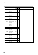
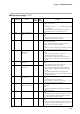
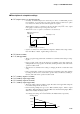
Table Of Contents
- CP-UM-5093E-04.pdf
- SAFETY PRECAUTIONS
- Contents
- Chapter 1. GENERAL
- Chapter 2. NAMES & FUNCTIONS OF PARTS
- Chapter 3. MOUNTING
- Chapter 4. WIRING
- 4-1 Wiring Precautions
- 4-2 Compensating Lead
- 4-3 Terminal Connections
- 4-4 Layout of Terminals and Recommended Lead Draw-out Direction
- 4-5 Connecting the Ground and Power Supply
- 4-6 Wiring of Standard and Add-on Terminal Base
- 4-7 Connecting Inputs (analog inputs)
- 4-8 Connecting control outputs (outputs 1, 2)
- 4-9 Connecting auxiliary outputs (outputs 2, 3)
- 4-10 Connecting Event Output (relay output)
- 4-11 Connecting Time Event Output (open-collector)
- 4-12 Connecting External Switch (RSW) Input
- 4-13 Connecting for Communications
- 4-14 Isolating Inputs and Outputs
- Chapter 5. FUNCTIONS
- Chapter 6. OPERATION
- Chapter 7. PARAMETER SETUP
- Chapter 8. PROGRAM SETUP
- Chapter 9. TROUBLESHOOTING
- Chapter 10. SPECIFICATIONS
- Chapter 11. CALIBRATION
- Index
Chapter 7. PARAMETER SETUP
7-35
● C 7 8 (voltage output 1 adjustment)
● C 7 q (voltage output 2 adjustment)
When driving an SSR by voltage time-proportional output, the output voltage of the
controller must be within the input rated voltage (optimum ignition voltage) of the SSR.
On the DCP301, a newly developed variable output system is utilized that enables output
of the optimum ignition voltage even when driving two or more SSRs.
This system sets the optimum current value on the controller so that the optimum ignition
voltage with respect to the internal impedance of the SSR side can be obtained.
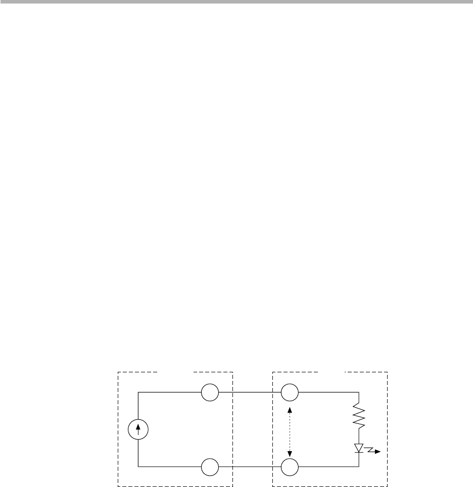
The following shows equivalent circuits and related formulas.
• Description of Symbols
(1) Details
IO : Setting output current of controller (setting range: 2 to 22mA)
VO : Maximum applied load voltage (approx. 14.7V)
VSSR’ : Actual input voltage to SSR
VSSR : Input rated voltage range of SSR (VSSR/MIN to VSSR/MAX)
VSSR/MIN : Minimum input rated voltage of SSR
VSSR/MAX : Maximum input rated voltage of SSR
Z : Internal impedance of SSR
VD : Internal voltage drop of SSR (normally 1 to 2V)
(2) Equivalent circuit when one SSR is connected
DCP301 SSR
+
–
+
–
I
O
(V
O
)
V
SSR'
Z
V
D
Formulas (1) and (2) formulas must be satisfied.
(1) formula VSSR/MIN ≤ IO x Z + VD ≤ VO
(2) formula VSSR' < VSSR/MAX
(VSSR' = IO x Z + VD)