AR-B7041 8MB/4MB SOLID STATE DISK User’ s Guide Edition: 1.3 Book Number: AR-B7041-99.
AR-B7041 User¡¦s Guide Table of Contents 0. PREFACE....................................................................................................................................................... 0-2 0.1 0.2 0.3 0.4 0.5 0.6 0.7 1. OVERVIEW..................................................................................................................................................... 1-1 1.1 1.2 1.3 2. COPYRIGHT NOTICE AND DISCLAIMER ...........................................................
AR-B7041 User¡¦s Guide 0.PREFACE 0.1 COPYRIGHT NOTICE AND DISCLAIMER September 1996 Acrosser Technology makes no representations or warranties with respect to the contents hereof and specifically disclaims any implied warranties of merchantability or fitness for any particular purpose.
AR-B7041 User¡¦s Guide 0.6 ORGANIZATION This information for users covers the following topics (see the Table of Contents for a detailed listing): l l l l l l Chapter 1, “Overview,” provides an overview of the system features and packing list. Chapter 2, “Installation,” describes the utility diskette using, solid state disk’ s writing protect function, and the watchdog timer.
AR-B7041 User¡¦s Guide 1. OVERVIEW This chapter provides an overview of your system features and capabilities. The following topics are covered: l l l Introduction Packing List Features 1.1 INTRODUCTION The AR-B7041 is a solid state disk card that can be used as the system disk or as a replacement for mechanical disk drives is any IBM PC/XT/AT or compatible computer.
AR-B7041 User¡¦s Guide 1.2 PACKING LIST The accessories are included with the system. Before you begin installing your AR-B7041 board, take a moment to make sure that the following items have been included inside the AR-B7041 package. l l l The quick setup manual 1 AR-B7041 solid state disk card 1 Software utility If you purchased an AR-B7017, please check that the following items have been included in the AR-B7017 package.
AR-B7041 User¡¦s Guide 2. INSTALLATION This chapter describes the procedure of the utility diskette installation. The following topics are covered: l l l l Overview Utility Diskette Write Protect Function Watchdog Timer 2.1 OVERVIEW This chapter provides information for you to set up a working system based on the AR-B7041 card. Please read the details of the card’ s hardware descriptions before installation carefully, especially jumpers’ setting, switch settings and cable connections.
AR-B7041 User¡¦s Guide Verify Memory If ROM pattern files were loaded without error, this option instructs PGM7041 to verify the contents of (FLASH) memory chips with the current ROM pattern files. Program Memory If there are no mistakes in your ROM pattern file, then this menu option will erase (FLASH) memory, write the current ROM pattern files onto (FLASH) memory and verify data that was just written to (FLASH) memory, using the ROM pattern files. Memory Type/Mfr.
AR-B7041 User¡¦s Guide Quit to DOS Quits and exits to the DOS OS Shell Exits from the RFG temporarily to the DOS prompt. Type to return to the RFG main menu. Load PFG File If this option is used, the RFG will prompt you for the PGF file name. This option is useful if you have not previously entered a PGF name or you wish to use a different PGF file.
AR-B7041 User¡¦s Guide An examples of the *.PGF file is as follow. ROM_NAME=TEST1 DOS_DRIVE=C: ROM_SIZE=128 ; ROM pattern file name is TEST1 ; The output file names will be TEST1.R01, TEST1.R02..etc.
AR-B7041 User¡¦s Guide 2.3.3 Enable the Software Write Protect Write 80h to the base port+0 address Example 1: (in assembly language) MOV DX, 220H MOV AL, 80H OUT DX, AL ; If the AR-B7041’ s base I/O address is 220H ; Enable byte = 80h Example 2: (in BASICA language) OUT &H220, &H80; REM If the AR-B7041’ s base I/O address is 220h Example 3: (in Turbo C language) outportb(0x220,0x80); /*If the AR-B7041’ s base I/O address is 220h*/ 2.3.
AR-B7041 User¡¦s Guide 2.4.1 Watchdog Timer Setting The watchdog timer is a circuit that may be used from your program software to detect crashes or hang-ups. Whenever the watchdog timer is enabled, the LED will blink to indicate that the timer is counting. The watchdog timer is automatically disabled after reset. Once you have enabled the watchdog timer, your program must trigger the watchdog timer every time before it times-out.
AR-B7041 User¡¦s Guide 2.4.4 Watchdog Timer Trigger After you enable the watchdog timer, your program must write the same factor as enabling to the watchdog register at least once every time-out period to its previous setting. You can change the time-out period by writing another timer factor to the watchdog register at any time, and you must trigger the watchdog before the new time-out period in next trigger.
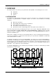
AR-B7041 User¡¦s Guide 3.SOLID STATE DISK The section describes the various type SSDs’ installation steps as follows. This chapter describes the procedure of the installation. The following topics are covered: l l l l l Overview Switch Setting Jumper Setting ROM Disk Installation AR-B7017 3.1 OVERVIEW Eight 32-pin JEDEC memory sockets on the AR-B7041 can be populated with up to 8MB of EPROM, 4MB of FLASH, 4MB of SRAM or combinations the EPROM/SRAM or FLASH/SRAM.
AR-B7041 User¡¦s Guide 3.2 SWITCH SETTING We will show the locations of the AR-B7041 switch, and the factory-default setting. CAUTION: The switch setting needs to adjust with the jumpers setting, make sure the jumper settings and the switch setting are correct.
AR-B7041 User¡¦s Guide 3.2.2 I/O Port Address Select (SW1-1 & SW1-2) SW1-1 and SW1-2 are provided to select one of the four base port addresses for the watchdog timer and the solid state disk. The AR-B7041 occupies 4 I/O port addresses. The following state selections of base port address. SW1-1 SW1-2 Base Port Solid State Disk Watchdog OFF (*) OFF 220h 220h-222h 223h & 76h-77h ON OFF 2A0h 2A0h-2A2h 2A3h & 76h-77h OFF ON 320h 320h-322h 323h ON ON 3A0h 3A0h-3A2h 3A3h Table 3-1 I/O Port Address Select 3.2.
AR-B7041 User¡¦s Guide NOTE: 1. Factory preset 2. If there is no DOS on this ROM/RAM disk, the disk number will be 1. If any DOS is found by the ARB7041 BIOS, the disk number will be 0. But, you can change the disk number from 0 to 1 by pressing key during system boot-up. 3. If there is no DOS on this SSD, the disk number will be 2 (C: or D: or …). If any DOS is found by ARB7041 SSD BIOS, the disk number will be 0 (A:).
AR-B7041 User¡¦s Guide (2) Disk Drive Name Arrangement If any logical hard disk drives exist in your system, there will also be a different disk number depending on which version DOS you are using. The solid state disk drive number with there respective DOS drive designation are listed in table as follows. The solid state disk drive number is changeable as the DOS version. The following table expresses the variety. Floppy disk No.
AR-B7041 User¡¦s Guide 3.3 JUMPER SETTING Jumper pins allow you to set specific system parameters. Set them by changing the pin location of jumper blocks. (A jumper block is a small plastic-encased conductor [shorting plug] that slips over the pins.) To change a jumper setting, remove the jumper from its current location with your fingers or small needle-nosed pliers. Place the jumper over the two pins designated for the desired setting. Press the jumper evenly onto the pins.
AR-B7041 User¡¦s Guide A B C JP1 1 2 3 M1, M2, M3, & M4 A B 1 2 3 1MX8 EPROM (Only) C JP1 1 2 1 2 3 3 M1, M2, M3, & M4 EPROM (128KX8, 256KX8 and 512KX8) 5V FLASH (64KX8, 128KX8 and 256KX8) (Factory Preset) A B C JP1 1 2 1 2 3 3 M1, M2, M3, & M4 A B 5V FLASH (512KX8 Only) C JP1 1 2 3 M1, M2, M3, & M4 1 2 3 SRAM Figure 3-3 M1~M4 & JP1: Memory Type Setting 3-7
AR-B7041 User¡¦s Guide 3.3.
AR-B7041 User¡¦s Guide 3.3.3 Battery Setting (1) Battery Charge Enable/Disable (JP2) If the AR-B7041 uses a 3.6V Ni-Cd rechargeable battery for SRAM data retention, the on-board charge circuit can be enabled by set the JP2 jumper. The battery will be charged when the power is on.
AR-B7041 User¡¦s Guide ON OFF 1 2 3 4 5 6 7 8 9 10 Figure 3-9 UV EPROM (27CXXX) Switch Setting A B C JP1 1 2 3 M1, M2, M3, & M4 A B 1 2 3 1MX8 EPROM (Only) C JP1 1 2 1 2 3 3 M1, M2, M3, & M4 EPROM (128KX8, 256KX8 and 512KX8) Figure 3-10 UV EPROM Jumper Setting (2) Software Programming Use the UV EPROM, please refer to the follow steps: Step 1: Turn on the power and boot DOS from hard disk drive or floppy disk drive. Step 2: Making a Program Group File (*.PGF file) Step 3: Using the RFG.
AR-B7041 User¡¦s Guide 3.4.2 Large Page 5V FLASH Disk If you are using large page 5V FLASH as ROM disk, it is the same procedure as step 1 to step 4 of using the UV EPROM. (1) Switch and Jumper Setting Step 1: Use jumper block to set the memory type as ROM (FLASH). Step 2: Select the proper I/O base port, firmware address, disk drive number and large page 5V FLASH type on SW1. Step 3: Insert programmed EPROM(s) or FLASH(s) chips into sockets starting at MEM1.
AR-B7041 User¡¦s Guide NOTE: The FLASH EPROM program is built-in the AR-B7041 board. The FLASH EPROMs can be programmed on the AR-B7041. Before programming the FLASH EPROMs, please insert at least the same number of FLASH EPROMs, please insert at least the same number of FLASH EPROMs, please insert at least the same number of FLASH chips as the ROM pattern files generated. Step 5: The PGM7041.EXE file is a program that loads and writes the ROM pattern files onto the (FLASH) memory chips.
AR-B7041 User¡¦s Guide A B C 1 2 3 JP1 1 2 3 5V/12V FLASH (64KX8M 128KX8, 256KX8) Factory Preset M1~M4 A B C 1 2 3 JP1 1 2 3 5V FLASH (512KX8 only) M1~M4 Figure 3-14 5V FLASH (29CXXX & 28EEXXX) Jumper Setting (2) Using Tool Program If small page 5V FLASH EPROMs are used, it is the same procedure as step 1 to step 4 of using the UV EPROM: Step 1: Making a Program Group File (*.
AR-B7041 User¡¦s Guide CAUTION: It is not recommended that the user formatted the disk and copy files to the FLASH disk very often. Since the FLASH EPROM’ s write cycle life time is about 10,000 or 100,000 times, writing data to the FLASH too often will reduce the life time of the FLASH EPROM chips, especially the FLASH EPROM chip in the MEM1 socket. 3.4.4 RAM Disk (1) Switch and Jumper Setting Step 1: Use jumper block to set the memory type as ROM (FLASH).
AR-B7041 User¡¦s Guide 3.4.5 Combination of ROM and RAM Disk The AR-B7041 can be configured as a combination of one ROM disk and one RAM disk. Each disk occupies a drive unit. Step 1: Use jumper block to select the proper ROM/RAM configuration you are going to use. Step 2: Insert the first programmed EPROM into the socket mem1, the second into the socket MEM2, etc. Step 3: Insert the SRAM chips starting from the first socket assigned as SRAM.
AR-B7041 User¡¦s Guide 3.5.1 Memory Type Setting (JP1 ~ JP4) The AR-B7017 provides 4 sockets for memory chips. l l l l JP1: is used to configure the memory type of MEM1 & MEM2 JP2: is used to configure the memory type of MEM3 & MEM4 JP3: is used to configure the memory type of MEM5 & MEM6 JP4: is used to configure the memory type of MEM7 & MEM8 CAUTION: When the power is turned off, please note the following precautions. 1.
AR-B7041 User¡¦s Guide (C) External Battery Supplied for SRAM Data Storage (JP7) JP7 1 2 3 External Battery 1 2 3 Internal Battery Figure 3-20 JP7: External Battery Supplied for SRAM Data Storage 3.5.3 Piggy-Back Connector (CN1) CN1 is used to connect with the AR-B7041.
AR-B7041 User¡¦s Guide 4. SPECIFICATIONS & SSD TYPES SUPPORTED 4.
AR-B7041 User¡¦s Guide 4.2 AR-B7017 Memory Socket: 8 Disk Capacity: Installation: EPROM – 4MB maximum FLASH – 4MB maximum SRAM – 4MB maximum Piggyback Accepts EPROM: 27C010 (128Kx8), 27C020 (256Kx8) and 27C040 (512Kx8) Accepts 5V FLASH: 64Kx8 to 512Kx8 (28EExxx, 28SFxxx, 29Cxxx, 29Fxxx or 29EExxx) Accepts SRAM: 581000 (128Kx8) and 584000 (512Kx8) External Battery: Provides connector for external battery Power Supply: +5V only Power Consumption: +5V DC+/- 5%, 0.
AR-B7041 User¡¦s Guide 4.
AR-B7041 User¡¦s Guide 4-4 NS SGS-THOMSON TI TOSHIBA NM27C020 M27C2001 TMS27C020 TCS712000 (256Kx8, 2M bits) (256Kx8, 2M bits) (256Kx8, 2M bits) (256Kx8, 2M bits) AMD ATMEL FUJITSU HITACHI INTEL MITSUBISHI NEC NS SGS-THOMSON TI TOSHIBA Am27C040 AT27C040 MBM27C4001 HN27C401 D27C040 M5M27C401 D27C4001 NM27C040 M27C4001 TMS27C040 TCS714000 (512Kx8, 4M bits) (512Kx8, 4M bits) (512Kx8, 4M bits) (512Kx8, 4M bits) (512Kx8, 4M bits) (512Kx8, 4M bits) (512Kx8, 4M bits) (512Kx8, 4M bits) (512Kx8, 4M bits) (512
AR-B7041 User¡¦s Guide 5. MEMORY BANKS & INDEX 5.1 USING MEMORY BANKS This chapter provides the information about how to access the memory on the AR-B7041 without using the ARB7041 SSD BIOS. The AR-B7041 hardware cut every 8K bytes of memory into a memory bank. To access the data in memory, you have to assign the chip number and the bank number. On every chip, the memory bank number starts from the number zero. The last memory bank number depends on the size of the memory chip used on the AR-7041.
AR-B7041 User¡¦s Guide CAUTION: BS0 to BS6 are the memory bank select bits. For example, 128KB memory has sixteen 8K-byte banks, so 4 bits (BS0 to BS3) are needed. Example 1: Select the 10th bank of the MEM4 on the AR-B7041. The AR-B7041 is using 27C020 (256K*8), and the base port is &H220. 100 base_port=&H220 110 OUT base_port+0,&H19 120 OUT base_port=1,&H13 Example 2: Select the last bank of MEM5 on the second AR-B7017 piggyback module.
AR-B7041 User¡¦s Guide The AR-B7041 provides 8 sockets for memory chips. Each AR-B7041 card also could be piggy-backed 1 ARB7017 to have more sockets for more memory capacity.
AR-B7041 User¡¦s Guide If you need to expand the memory capacity, you should install one AR-B7017 on the CN1 piggy-back connector of the first AR-B7041. The following table shows the locations and sequence of all AR-B7041 and AR-B7017 sockets.
AR-B7041 User¡¦s Guide 5.
AR-B7041 User¡¦s Guide 6. PLACEMENT & DIMENSIONS 6.
AR-B7041 User¡¦s Guide (2) AR-B7017 CN1 1 2 3 RAM ROM H1 JP1 HJ2 HJ3 HJ4 HJ1 U6 MEM4 U5 MEM3 U4 MEM2 U3 MEM1 U10 MEM8 U9 MEM7 U8 MEM6 U7 MEM5 - + 1 JP2 2 3 JP5 JP7 - + - + 6-2 JP6 1 2 3 RAM JP4 ROM 1 2 3 JP3 HJ8 HJ5 HJ7 HJ6 H2
AR-B7041 User¡¦s Guide 6.2 DIMENSIONS FOR AR-B7041 6895 6750 4100 3850 210 1890 95 3190 905 940 Unit: mil (1 inch = 25.