
User Manual


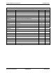


Table Of Contents
- Overview
- Hardware Description
- System Requirements
- Desktop Test Set-up
- Hardware Configuration
- WinCE Test Setup
- HCI Test Setup
- Suspend\Resume
- Bluetooth Driver List
- Certification Testing Utilities
- KwikBlue Development Board Jumpers
- Audio CODEC Setup (Optional)
- KwikBlue Development Board Bill of Materials (BOM)
- CODEC Board Bill of Materials (BOM)
- Errata
- Appendix A: BC01 vs. BC02 Pin Assignments

KwikBlue Module Development Kit Installation Guide
BC01 Class 1 Module Pin Assignments
Signal Name Function Direction Pin #
GROUND Ground 1
PCM_OUT PCM data stream output OUT 2
PCM_IN PCM data stream input IN 3
PCM_PWR_DWN PCM power down control output OUT 4
VBUS_IN For self-power mode, sense if VBUS is ON IN 5
UART_RXD UART/RxD from DTE IN 6
UART_TXD UART/TxD to DTE OUT 7
RESET System reset IN 8
USB_WAKE Wake up host when events occur during Suspend/Resume OUT 9
VCC Power supply 10
GROUND Ground 11
UART_RTS UART/Ready to send to DTE OUT 12
USB_DETACH Disconnect D+/D- from host IN 13
UART_CTS UART/Clear to send from DTE IN 14
PCM_SYNC PCM frame sync input/output (8 KHz) OUT 15
USB_D+ Positive USB differential data bus IN/OUT 16
USP_D- Negative USB differential data bus IN/OUT 17
PCM_CLK PCM reference clock input/output (256 KHz) OUT 18
NC For internal test use NC 19
VCC_PA Power supply 20
Table 7: BC01 Class 1 Module Pin Assigments
April 23, 2004 Copyright © 2003-2004 Socket Communications, Inc. Page 24
Document#: 6410-00215-C CONFIDENTIAL Revision 1.04