
- Standard Microsystems Hi-Speed USB Device Specification Sheet

Hi-Speed USB Device PHY with UTMI Interface
Datasheet
Revision 1.5 (11-15-07) 14 SMSC USB3280
DATASHEET
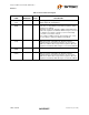
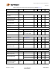
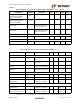
Table 6.3 DC Electrical Characteristics: Analog I/O Pins (DP/DM) (Note 6.3)
PARAMETER SYMBOL CONDITIONS MIN TYP MAX UNITS
FS FUNCTIONALITY
Input levels
Differential Receiver Input
Sensitivity
V
DIFS
| V(DP) - V(DM) | 0.2 V
Differential Receiver
Common-Mode Voltage
V
CMFS
0.8 2.5 V
Single-Ended Receiver Low
Level Input Voltage
V
ILSE
0.8 V
Single-Ended Receiver High
Level Input Voltage
V
IHSE
2.0 V
Single-Ended Receiver
Hysteresis
V
HYSSE
0.050 0.150 V
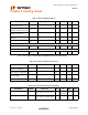
Output Levels
Low Level Output Voltage V
FSOL
Pull-up resistor on DP;
R
L
= 1.5kΩ to V
DD3.3
0.3 V
High Level Output Voltage V
FSOH
Pull-down resistor on DP,
DM;
R
L
= 15kΩ to GND
2.8 3.6 V
Termination
Driver Output Impedance for
HS and FS
Z
HSDRV
Steady state drive
(See Figure 6.1)
40.5 45 49.5 Ω
Input Impedance Z
INP
TX, RPU disabled 10 MΩ
Pull-up Resistor Impedance Z
PU
Bus Idle 0.900 1.24 1.575 kΩ
Pull-up Resistor Impedance Z
PURX
Device Receiving 1.425 2.26 3.09 kΩ
Termination Voltage For Pull-
up
Resistor On Pin DP
V
TERM
3.0 3.6 V
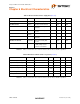
HS FUNCTIONALITY
Input levels
HS Differential Input Sensitivity V
DIHS
| V(DP) - V(DM) | 100 mV
HS Data Signaling Common
Mode Voltage Range
V
CMHS
-50 500 mV
HS Squelch Detection
Threshold (Differential)
V
HSSQ
Squelch Threshold 100 mV
Unsquelch Threshold 150 mV
Output Levels
High Speed Low Level
Output Voltage (DP/DM
referenced to GND)
V
HSOL
45Ω load -10 10 mV