
- Standard Microsystems Hi-Speed USB Device Specification Sheet

Hi-Speed USB Device PHY with UTMI Interface
Datasheet
Revision 1.5 (11-15-07) 10 SMSC USB3280
DATASHEET
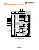
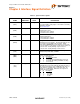
Table 4.2 Data Interface Signals
NAME DIRECTION
ACTIVE
LEVEL DESCRIPTION
DATA[7:0]
(D7)
.
.
.
(D0)
Bidirectional High Data bus. 8-bit Bidirectional mode.
TXVALID DATA[7:0]
0 output
1 input
TXVALID
(TXV)
Input High Transmit Valid. Indicates that the DATA bus is valid for transmit. The
assertion of TXVALID initiates the transmission of SYNC on the USB
bus. The negation of TXVALID initiates EOP on the USB.
Control inputs (OPMODE[1:0], TERMSELECT,XCVRSELECT) must
not be changed on the de-assertion or assertion of TXVALID. The
PHY must be in a quiescent state when these inputs are changed.
TXREADY
(TXR)
Output High Transmit Data Ready. If TXVALID is asserted, the SIE must always
have data available for clocking into the TX Holding Register on the
rising edge of CLKOUT. TXREADY is an acknowledgement to the
SIE that the transceiver has clocked the data from the bus and is
ready for the next transfer on the bus. If TXVALID is negated,
TXREADY can be ignored by the SIE.
RXVALID
(RXV)
Output High Receive Data Valid. Indicates that the DATA bus has received valid
data. The Receive Data Holding Register is full and ready to be
unloaded. The SIE is expected to latch the DATA bus on the rising
edge of CLKOUT.
RXACTIVE
(RXA)
Output High Receive Active. Indicates that the receive state machine has
detected Start of Packet and is active.
RXERROR
(RXE)
Output High Receive Error.
0: Indicates no error.
1: Indicates a receive error has been detected.
This output is clocked with the same timing as the receive DATA lines
and can occur at anytime during a transfer.
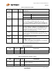
Table 4.3 USB I/O Signals
NAME DIRECTION
ACTIVE
LEVEL DESCRIPTION
DP I/O N/A USB Positive Data Pin.
DM I/O N/A USB Negative Data Pin.
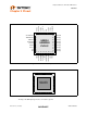
Table 4.4 Biasing and Clock Oscillator Signals
NAME DIRECTION
ACTIVE
LEVEL DESCRIPTION
RBIAS
(RB)
Input N/A External 1% bias resistor. Requires a 12kΩ resistor to ground.
Used for setting HS transmit current level and on-chip
termination impedance.
XI/XO Input N/A External crystal. 24MHz crystal connected from XI to XO.