
user manual

10/100 Non-PCI Ethernet Single Chip MAC + PHY
Datasheet
SMSC LAN91C111 REV C 55 Revision 1.91 (08-18-08)
DATASHEET
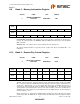
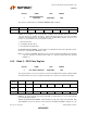
8.12 Bank 1 - Base Address Register
This register holds the I/O address decode option chosen for the LAN91C111. It is part of the EEPROM
saved setup and is not usually modified during run-time.
A15 - A13 and A9 - A5 - These bits are compared against the I/O address on the bus to determine
the IOBASE for the LAN91C111‘s registers. The 64k I/O space is fully decoded by the LAN91C111
down to a 16 location space, therefore the unspecified address lines A4, A10, A11 and A12 must be
all zeros.
All bits in this register are loaded from the serial EEPROM. The I/O base decode defaults to 300h
(namely, the high byte defaults to 18h).
Reserved – Reserved bits.
Below chart shows the decoding of I/O Base Address 300h:
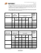
8.13 Bank 1 - Individual Address Registers
These registers are loaded starting at word location 20h of the EEPROM upon hardware reset or
EEPROM reload. The registers can be modified by the software driver, but a STORE operation will not
modify the EEPROM Individual Address contents. Bit 0 of Individual Address 0 register corresponds
to the first bit of the address on the cable.
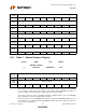
OFFSET NAME TYPE SYMBOL
2
BASE ADDRESS
REGISTER READ/WRITE BAR
HIGH
BYTE
A15A14A13A9A8A7A6A5
00011000
LOW
BYTE
Reserved Reserved
00000001
A15 A14 A13 A12 A11 A10 A9 A8 A7 A6 A5 A4 A3 A2 A1 A0
0000001100000000
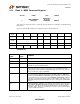
OFFSET NAME TYPE SYMBOL
4
THROUG
H 9
INDIVIDUAL ADDRESS
REGISTERS READ/WRITE IAR