
user manual
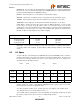

10/100 Non-PCI Ethernet Single Chip MAC + PHY
Datasheet
Revision 1.91 (08-18-08) 46 SMSC LAN91C111 REV C
DATASHEET
Regardless of the functional description, all registers can be accessed as doublewords, words or bytes.
The default bit values upon hard reset are highlighted below each register.
A special BANK (BANK7) exists to support the addition of external registers.
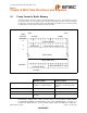
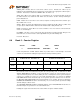
8.4 Bank Select Register
BS2, BS1, BS0 Determine the bank presently in use. This register is always accessible and is used
to select the register bank in use.
The upper byte always reads as 33h and can be used to help determine the I/O location of the
LAN91C111.
The BANK SELECT REGISTER is always accessible regardless of the value of BS0-2
Note: The bank select register can be accessed as a doubleword at offset 0x0Ch, as a word at offset
0x0Eh, or as a byte at offset 0x0Eh, A doubleword write to offset 0x0Ch will write the BANK
SELECT REGISTER but will not write the registers 0x0Ch and 0x0Dh, but will only write to
register 0x0Eh
BANK 7 has no internal registers other than the BANK SELECT REGISTER itself. On valid cycles
where BANK7 is selected (BS0=BS1=BS2=1), and A3=0, nCSOUT is activated to facilitate
implementation of external registers.
Note: BANK7 does not exist in LAN91C9x devices. For backward S/W compatibility BANK7 accesses
should be done if the Revision Control register indicates the device is the LAN91C111.
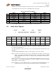
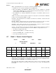
Table 8.1 Internal I/O Space Mapping
BANK0 BANK1 BANK2 BANK3
0 TCR CONFIG MMU COMMAND MT0-1
2 EPH STATUS BASE PNR MT2-3
4 RCR IA0-1 FIFO PORTS MT4-5
6 COUNTER IA2-3 POINTER MT6-7
8 MIR IA4-5 DATA MGMT
A RPCR GENERAL PURPOSE DATA REVISION
C RESERVED CONTROL INTERRUPT RCV
E BANK BANK BANK BANK
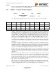
OFFSET NAME TYPE SYMBOL
E BANK SELECT REGISTER READ/WRITE BSR
HIGH
BYTE
Reserved Reserved Reserved Reserved Reserved Reserved Reserved Reserved
00110011
LOW
BYTE
BS2 BS1 BS0
XXXXX000