AN 9.6 SMSC LAN91C111 32/16/8-Bit Three-InOne Fast Ethernet Controller Technical Reference Manual 1 Overview This Technical Reference Manual provides detailed part-specific information and general system design guidelines for the SMSC LAN91C111. Hardware engineers and software engineers should be familiar with this material before interfacing the SMSC LAN91C111 to a microprocessor or microcontroller. This Manual is an active document and will be updated as required.
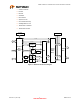
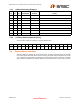
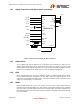
SMSC LAN91C111 32/16/8-Bit Three-In-One Fast Ethernet Controller Collision Detection Encoder Decoder Scrambler De-scrambler Squelch Circuits Clock & Data Recovery AutoNegotiation & Link Twisted Pair Transmitter Twisted Pair Receiver EEPROM INTERFACE MII Control Control Control Arbiter Control Address 8-32 bit Bus Interface Unit Control Control TPO Control WR FIFO Data RD FIFO MMU Ethernet Protocol Handler (EPH) DMA TX/RX FIFO Pointer TX Data 8K Byt
SMSC LAN91C111 32/16/8-Bit Three-In-One Fast Ethernet Controller 3 Description Of Bus Interface Unit (BIU) This section is intended to aid design engineers connecting the SMSC LAN91C111 device to a microprocessor or microcontroller. This section will discuss in detail the functional block, and the individual control signals of the LAN91C111 involved in the connection between the device and an associated microprocessor / microcontroller. 3.
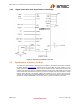
SMSC LAN91C111 32/16/8-Bit Three-In-One Fast Ethernet Controller Figure 3.1 BIU Section of functional Block Diagram For those interested in designing connected to an ISA bus, SMSC provides both a reference design and evaluation board. Please contact your SMSC Sales Representative or Distributor for information regarding either of these products. The Data Sheet also contains block diagrams of a typical ISA, EISA, and VL-Bus based designs. 3.
SMSC LAN91C111 32/16/8-Bit Three-In-One Fast Ethernet Controller 3.3.
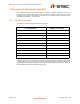
SMSC LAN91C111 32/16/8-Bit Three-In-One Fast Ethernet Controller 3.4.1 Typical Signal Connection with Asynchronous Buses HOST SIGNALS LAN91C111 SIGNALS A1-A15 A1-A15 Address D0-D31 D0-D31 Data nBE [0-3] nBE[0-3] Byte Enable AEN/CS AEN Active low address enable. It can be connected to ship select if the chip select timing matches to AEN Reset Reset Reset nADS/Ground nADS Active low address latch signal. It can be tied low, please see the timing diagrams figure 24 to 26 of the database.
SMSC LAN91C111 32/16/8-Bit Three-In-One Fast Ethernet Controller 3.4.2 Signal Connection with Asynchronous Interfacing Figure 3.2 Asynchronous Interface Connection 3.5 Synchronous Interface (VL-Bus) The LAN91C111 also supports a 32-bit synchronous interface. This interface is intended to duplicate the VESA standard (www.vesa.org), otherwise known as the VL-Bus. Since this interface is not as widely understood as the ISA bus we will go over this interface in some detail in this document.
SMSC LAN91C111 32/16/8-Bit Three-In-One Fast Ethernet Controller 3.5.1 Typical Connection with Synchronous Interface (VL-Bus) HOST (VL BUS) SIGNAL LAN91C111 SIGNAL A2-A15 A2-A15 M/nIO AEN Qualifies valid I/O decoding - enabled access when low. This signal is latched by nADS rising edge and transparent on nADS low time. W/nR W/nR Direction of access. Sampled by the LAN91C111 on first rising clock that has nCYCLE active. High on writes, low on reads.
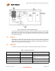
SMSC LAN91C111 32/16/8-Bit Three-In-One Fast Ethernet Controller 3.5.2 Signal Connection with Synchronous Interfacing +VCC W/nR W/nR A2-A15 A2-A15 LCLK LCLK M/nIO AEN nR D nWR A1 nVLBUS nDATACS LAN91C111 IRQn INTR0 D0-D31 D0-D31 nRDYRTN nRDYRTN nBE0-nBE3 nBE0-nBE3 nADS nADS nCYCLE delay1 nLRDY (Open) RESET nRESET nSRDY O.C. simulated O.C. nLDEV nLDEV Figure 3.3 Synchronous Interface (VL-Bus) Connection 3.5.3 Address Bus The 13 address lines form the address bus.
SMSC LAN91C111 32/16/8-Bit Three-In-One Fast Ethernet Controller 3.5.6 NRDYRTN Ready Return is an input signal generated by the host controller to establish a handshake signal to inform the LAN91C111 that the cycle has ended. For LCLK speeds up to 33Mhz, nRDYRTN is typically asserted in the same LCLK cycle as nSRDY is asserted. For higher LCLK speed, nRDYRTN may trail nSRDY by one LCLK cycle due to signal resynchronization.
SMSC LAN91C111 32/16/8-Bit Three-In-One Fast Ethernet Controller 3.5.11 32-Bit Access and nBE0-nBE3 The LAN91C111 can operate in 32, 16, or 8-bit mode. Since the registers are assigned to different banks, changing bank is required if accessing to registers at other bank.
SMSC LAN91C111 32/16/8-Bit Three-In-One Fast Ethernet Controller t23 t20 t24 t10 Clock t9 Address, AEN, nBE[3:0] Valid t8 nADS t16 W/nR t11 nCYCLE Read Data Valid t21 t21 nSRDY nRDYRTN Figure 3.
SMSC LAN91C111 32/16/8-Bit Three-In-One Fast Ethernet Controller accomplished through external circuitry. Signal W/nR has to be asserted high no later than nCYCLE assertion. 3.6.2 Write Cycle Data Phase - Cycle End During next rising edge after de-assertion of nCYCLE, write data has to be presented to the LAN91C111. The data bus will need to be stable at least 15nS prior to the rising edge of LCLK and are required to hold 4nS, as specified by timing parameter t18 and t20.
SMSC LAN91C111 32/16/8-Bit Three-In-One Fast Ethernet Controller 3.6.
SMSC LAN91C111 32/16/8-Bit Three-In-One Fast Ethernet Controller 3.7.1 The Use of NDATACS Direct access to the Data Register is controlled via the nDATACS pin. This is can be accomplished whether the LAN91C111 is configured for synchronous or asynchronous operations. Accessing the LAN91C111 via the nDATACS pin bypasses the internal Bus Interface Unit (BIU) decoders and accesses designated by the nDATACS are steered towards the Data Register only.
SMSC LAN91C111 32/16/8-Bit Three-In-One Fast Ethernet Controller READ When set (1) the operation is a read; when cleared (0) the operation is a write. NOT EMPTY This read-only bit indicates whether the Write Data FIFO is empty or not. The FIFO is not empty when this bit is set. POINTER HIGH These bits comprise the upper three bits of the address. POINTER LOW These bits comprise the lower 8-bits of the address.
SMSC LAN91C111 32/16/8-Bit Three-In-One Fast Ethernet Controller t2 nDATACS t3A t4 Read Data Valid t6A t1 t5 nRD, nWR t5A Write Data D0-D31 Valid Figure 3.
SMSC LAN91C111 32/16/8-Bit Three-In-One Fast Ethernet Controller nRDYRTN can be used to insert wait states. In Synchronous mode back to back time between read or write is limited by access times. From timing diagram, it is 3 clocks for read and 2 clocks for write, but it has to be bigger than 100ns for read and 80ns for write. 3.10 Burst Mode Write Operation The timing diagram below details a burst mode write operation and shows three separate packets of data being transferred.
SMSC LAN91C111 32/16/8-Bit Three-In-One Fast Ethernet Controller This timing diagram examples and details a burst mode write operation. The nDATACS pin remains asserted throughout the cycle and the nCYCLE pin is used to control the burst data. As long as nCYCLE remains asserted, data can be written on each rising edge of LCLK. In the above timing diagram nRDYRTN is used to insert a wait state between the second and third data packet.
SMSC LAN91C111 32/16/8-Bit Three-In-One Fast Ethernet Controller PARAMETER MIN TYP MAX UNITS t15 nRDYRTN Hold after LCLK Falling 10 ns t17 W/nR Setup to LCLK Falling 15 ns t17A W/nr Hold After LCLK Falling 3 ns Data Delay from LCLK Rising (Read) 5 t19 15 ns As you can see by the timing diagram and subsequent timing parameter table the nDATACS signal is used to indicate that the cycle is a burst mode direct operation.
SMSC LAN91C111 32/16/8-Bit Three-In-One Fast Ethernet Controller SIGNAL NAME BRIEF DESCRIPTION LCLK Clock Input W/nR Read or Write operation, Read active low nRDYRTN Used to insert wait states OPTIONAL SIGNALS nDATACS Direct access 32-bit mode operation nCYCLE Used to indicate Burst operation From the table listed above, the interface is capable of multiple types of connections.
SMSC LAN91C111 32/16/8-Bit Three-In-One Fast Ethernet Controller Remote End Ping to LAN91C111 Routine P ing th e LA N91 C11 1 Fro m Remo te En d Ho st P roce ssed Data & Se nt Tran smit Req ue st to Dri ve r 1 10 LA N91 C111 Receive d the First Fram e Driver A llo cated o ne P ag e of the LA N91C1 11 B uffer for Tr ansm it 2 11 Star te d to Tran smit Data fro m Host M em o ry to th e L AN9 1C1 11 Inte rna l Bu ffer LA N91 C11 1 Ge ne rates a n In terru pt Requ est to Ho st 3 12 Com ple tely Tran
SMSC LAN91C111 32/16/8-Bit Three-In-One Fast Ethernet Controller 4 System Hardware Design The LAN91C111 fully integrates the MAC, PHY, and SRAM into a single chip. It requires a minimum number of external components to complete the system design. For example, it requires only a transformer, an oscillator, some resistors, capacitors, and an optional EEPROM to complete a standard ISA system design.
SMSC LAN91C111 32/16/8-Bit Three-In-One Fast Ethernet Controller LIMIT SYMBOL PARAMETER MIN. TYPICAL MAX. UNIT t2 Xtal1 High Time 18 ns t3 Xtal1 Low time 18 ns It‘s not recommend to implement PLL clock parts with LAN91C111. The device is very sensitive to PLL clock jitters, which may cause startup and link problems. 4.2 Clock Oscillator If an external clock is used, it should be connected to the input of the amplifier (XTAL1). If an oscillator is to be used, leave XTAL2 floating.
SMSC LAN91C111 32/16/8-Bit Three-In-One Fast Ethernet Controller these parameters. In this way, many identical boards can be plugged into the same system by simply changing the IOS strapping. An additional feature of the LAN91C111 is the ability to change the EEPROM data while in circuit. Even if the EEPROM was not programmed initially you still have the ability to program the EEPROM via software. This feature also allows the reprogramming of a previously programmed EEPROM as well.
SMSC LAN91C111 32/16/8-Bit Three-In-One Fast Ethernet Controller Note: If no EEPROM is connected to the LAN91C111 the ENEEP pin should be grounded and no accesses to the EEPROM will be attempted. Configuration, Base, and Individual Address assume their default values upon hardware reset and the CPU is responsible for programming them for their final value. Table 4.1 EEPROM MEMORY MAP 4.4.
SMSC LAN91C111 32/16/8-Bit Three-In-One Fast Ethernet Controller In an ISA like application, system designers can have the choices of always using the chip at 300h, or having the controlling software access the base address registers at 300h and change it to other I/O address after accessing the chip at that address. Similarly for the other values usually stored in the EEPROM, the driver will have to load them at software initialization.
SMSC LAN91C111 32/16/8-Bit Three-In-One Fast Ethernet Controller The typical currents measured at the Vcc pins without pullup resistors on the transmit and receive circuits (Idle condition is defined as state of the chip after powerup (no reset issued), with no link established): Approximately 73 mA in the idle state after power up and before reset; Approximately 100 mA at 100 Mbps, and, approximately 73 mA at 10 Mbps, the typical measured current was approximately 8 mA in Power down mode, For details of t
SMSC LAN91C111 32/16/8-Bit Three-In-One Fast Ethernet Controller Table 4.3 - LAN91C111 Manual Configuration Mode Register Bill Settings AUTONEGOTIATION CONTROL BITS WHAT DO YOU WANT TO DO? Try to Manually Set to...... 100 Full Duplex 100 Half Duplex 10 Full Duplex 10 Half Duplex 4.7.
SMSC LAN91C111 32/16/8-Bit Three-In-One Fast Ethernet Controller A power up Auto-Negotiation enable initialization sequence is provided below for your reference: 1. Power up the chip. 2. Wait for 50ms. 3. Reset the chip by setting and clearing the SOFT_RST bit in the Receive Control Register. (Write 0x8000, then write 0x0000) 4. Wait for 50ms. 5. Set the ANEG bit to 1 in the Receive/PHY Control Register (MAC Register, Bank 0, Offset A) to enable the Auto_Negotiation mode. 6.
SMSC LAN91C111 32/16/8-Bit Three-In-One Fast Ethernet Controller 4.8 Power up / Initialization and Powerdown Mode When the LAN91C111 powers up or resets, the internal PHY enters the following modes. 1. Isolation Mode 2. Manual Mode (AutoNegotiation Off) 3. 10Mbps 4. Half Duplex When the internal PHY is placed in isolation mode, the internal PHY is able to respond to management transactions, such as reading / writing the PHY registers.
SMSC LAN91C111 32/16/8-Bit Three-In-One Fast Ethernet Controller 4.9.2 Diagnostic Loopback Setting the LPBK bit in the internal PHY MI serial port Control Register can enable diagnostic loopback mode. When diagnostic loopback is enabled, transmitted data at the internal MII is looped back into receive data output of the internal MII. The transmit enable signal is looped back into carrier sense output at the internal MII level. The TP receive and transmit paths are disabled.
SMSC LAN91C111 32/16/8-Bit Three-In-One Fast Ethernet Controller crossing the MII interface (internal to the 91C111). The loopback at point C is referred to as an external loopback, which loops the packet back after leaving the PHY and the external magnetics. This final type of loopback testing allows the design engineer to complete the circuit to ensure proper operation of their design.
SMSC LAN91C111 32/16/8-Bit Three-In-One Fast Ethernet Controller External Loopback: The packet is sent out of the MAC, through the PHY, out of the RJ45 connector and then looped back through external wiring or relay. In this mode the MAC and PHY must always be set for full duplex, since the transmitted packet will start to be received before it is completely out on the wire.
SMSC LAN91C111 32/16/8-Bit Three-In-One Fast Ethernet Controller 4.
SMSC LAN91C111 32/16/8-Bit Three-In-One Fast Ethernet Controller 6 Big and Little Endian Issues on the LAN91C111 6.1 Introduction The LAN91C111 is designed as a Little Endian architecture device. In order to accommodate the use of this device on Big Endian architectures there needs to be an understanding of these implications. This application note is intended to discuss the use of the LAN91C111 on Big Endian type architecture and the requirements that they may pose. 6.
SMSC LAN91C111 32/16/8-Bit Three-In-One Fast Ethernet Controller Table 6.2 Little Endian Memory Images Double Word Value to be Stored = 12345678h BYTE ADDRESS 3 2 1 0 DATA VALUES (H) 12 34 56 78 BINARY VALUES 0001 0010 0011 0100 01010110 0111 1000 The Intel 80X86 and Pentium and DEC Alpha RISC processors are Little Endian. 6.2.3 Bi-Endian As previously stated, some processors have the ability to switch their modes of operation to accommodate different endian structures.
SMSC LAN91C111 32/16/8-Bit Three-In-One Fast Ethernet Controller Figure 6.1 Byte Lane Configuration Revision 1.0 (08-14-08) 38 APPLICATION NOTE SMSC AN 9.
SMSC LAN91C111 32/16/8-Bit Three-In-One Fast Ethernet Controller Figure 6.2 16-bit Byte Lane Configuration As you can see the lower byte lane (Byte Lane 0) on the LAN91C111 becomes the upper byte lane on the processor. The second byte lane (Byte Lane 1) becomes the lower byte of the upper word on a 32bit interface. The third byte lane (Byte Lane 2) becomes the upper byte of the lower word on a 32bit interface and the upper byte on a 16bit interface.
SMSC LAN91C111 32/16/8-Bit Three-In-One Fast Ethernet Controller As with any software problem, there are many ways to accomplish this task. One method would be to have a routine that swaps the bytes around prior to outputting them to the LAN91C111. Another method might be too use a simple #define statement for each byte within a header file with the understanding of how they are configured and how the output needs to be accomplished.
SMSC LAN91C111 32/16/8-Bit Three-In-One Fast Ethernet Controller This example has extra stuff for defining the different architectures, but the key example is the byte swapping part at the bottom: /* * Little endian <==> big endian 32-bit swap macros.
SMSC LAN91C111 32/16/8-Bit Three-In-One Fast Ethernet Controller 6.6.1 Conclusion Given the flexibility of the LAN91C111 and with some creative software, the LAN91C111 can be connected to controllers other than Little Endian types. 7 Physical Layer and Magnetics 7.1 Transmit / Receive Interface The interface between the Twisted Pair outputs & the Twist Pair inputs on the LAN91C111 and the twisted pair cable is typically transformer coupled and terminated with the appropriate resistors. 7.1.
SMSC LAN91C111 32/16/8-Bit Three-In-One Fast Ethernet Controller The receive input must be terminated with the correct termination resistance to meet the input impedance and return loss requirements of IEEE 802.3. In addition, the receive TP inputs must be attenuated. Both the termination and attenuation is accomplished with four external resistors in series across the TPI± inputs.
SMSC LAN91C111 32/16/8-Bit Three-In-One Fast Ethernet Controller A better way to adjust the TP output level is to use the Transmit Level Adjust register bits (TLVL [3:0]) accessed through the MI serial port Configuration 1 register. These four bits can adjust the output level by -14% to +16% in 2% steps. 7.2.3 Cable Selection The LAN91C111 can drive two different cable types: 100 Ohm unshielded twisted-pair, Category 5, or 150 Ohm shielded twisted-pair.
SMSC LAN91C111 32/16/8-Bit Three-In-One Fast Ethernet Controller Timing and framing for each management command is to be generated by the CPU (host). For the MII Serial Frame Structure, please see 7.5.3 of the LAN91C111 datasheet. The PHY register set consists of eleven registers. The Control Register and the Status Register are the Basic Registers defined in the IEEE specification. The basic and fundamental control and status functions are defined in these two registers.
SMSC LAN91C111 32/16/8-Bit Three-In-One Fast Ethernet Controller outport(0x308, 0x333D);\ outport(0x308, 0x3339); #define WriteZToPhy \ outport(0x308, 0x3330);\ outport(0x308, 0x3334);\ outport(0x308, 0x3330); void WriteToPhyReg(char RegNo, int Data) { BankSelect(3); //Write atleast 32 1's to Synchronize the interface.
SMSC LAN91C111 32/16/8-Bit Three-In-One Fast Ethernet Controller { if (Data & 0x8000) { WriteOneToPhy;} else { WriteZeroToPhy;} Data <<= 1; } outport(0x308, 0x3330); return; } int ReadMDI() { int i; BankSelect(3); outport(0x308, 0x3330); outport(0x308, 0x3334); i = inport(0x308); outport(0x308, 0x3330); if (i & 0x0002) { return 1; } else { return 0; } } int ReadFromPhyReg(char RegNo) { int Data=0, binvalue, j; BankSelect(3); //Write atleast 32 1's to Synchronize the interface.
SMSC LAN91C111 32/16/8-Bit Three-In-One Fast Ethernet Controller WriteZeroToPhy WriteZeroToPhy WriteZeroToPhy //phy reg to read.. 5 bits..MSB First for (i=0; i<5; i++) { if (RegNo & 0x10) {WriteOneToPhy;} else {WriteZeroToPhy;} RegNo <<= 1; } //Send the turnaround bit WriteZToPhy; Data = 0; for (i=0; i<=15; i++) { Data <<= 1; if (ReadMDI()) Data |= 0x0001; } //Send the turnaround bit. WriteZToPhy; return Data; } main() { BankSelect(0); printf("\n\n\nResetting...
SMSC LAN91C111 32/16/8-Bit Three-In-One Fast Ethernet Controller outport(0x300, 0xA0B1); //Make sure the internal phy is selected //Now read the first register of the PHY BankSelect(3); for (int i=0; i<=5; i++) { printf("\nPHY Reg %d = 0x%04x", i, ReadFromPhyReg(i)); } //Write and read back different values.. to a PHY register... //We chose to R/W the ANEG advertisement register..
SMSC LAN91C111 32/16/8-Bit Three-In-One Fast Ethernet Controller 8 Reset Operation The LAN91C111 can be reset by either hardware or software. A hardware reset can be accomplished by asserting the RESET pin during normal operation, or upon powering up the device. This input is not considered active unless it is active for at least 100ns to filter narrow glitches. Both the MAC and the internal PHY are reset if a hardware reset is performed.
SMSC LAN91C111 32/16/8-Bit Three-In-One Fast Ethernet Controller Write the pointer register (bank 2, offset 6) = 0x0000 + J * 2 (RCV=0, AUTOINC=0, Read=0, Reserved=0, pointer=0x0000+J * 2) Write DATA register (bank 2 offset 8) = data word End Loop J Loop for J = 0 to 1023 (total of 1024 words of data) Write the pointer register (bank 2, offset 6) = 0x2000+ J * 2 (RCV=0, AUTOINC=0, Read=1, Reserved=0, pointer=0x20000+J * 2) Read DATA register (bank 2 offset 8) = data word Compare data word read with previou
SMSC LAN91C111 32/16/8-Bit Three-In-One Fast Ethernet Controller ** The packet will now be sent on the wire when the line is clear ** Poll for completion (<= 100ms) Read the INTERRUPT register until bit 1 (TX INT) is set (bank 2, offset C) Read the status word of the packet Write 0x6000 to the POINTER register (TX, RD, AUTOINC), (bank 2, offset 6) Read the DATA register (bank 2, offset 8) to get the Status Word of the packet The Status Word will show any errors in transmission; it mirrors the EPH STATUS re
SMSC LAN91C111 32/16/8-Bit Three-In-One Fast Ethernet Controller 9.7 EPH Loopback Test The following steps will transmit a packet and loop it back through the EPH (Ethernet Protocol Handler) block and back to the MAC.
SMSC LAN91C111 32/16/8-Bit Three-In-One Fast Ethernet Controller 9.10 MMU Test The MMU test is broken down into a series of tests that check each command of the MMU. 1.
SMSC LAN91C111 32/16/8-Bit Three-In-One Fast Ethernet Controller Write a 0x0080 to the MMUCOM register (bank 2, offset 0) The FIFO register should equal 0x0300 The MIR register should equal 0x0104 Write a 0x0080 to the MMUCOM register The FIFO register should equal 0x8300 The MIR register should equal 0x0204 The test fails if the EPH Loopback fails or the MIR or FIFO registers are incorrect. 5.
SMSC LAN91C111 32/16/8-Bit Three-In-One Fast Ethernet Controller Poll for TX INT Read the INTERRUPT register (bank 2, offset C) until bit 1 (TX INT) is set (< 100ms) End loop I The test fails if the allocation fails, the MIR register is incorrect, or the TX INT bit was not set for any packet within 100ms. 7. RESET TX FIFO’s Perform Section 9.
SMSC LAN91C111 32/16/8-Bit Three-In-One Fast Ethernet Controller 10.2 New Features and Modification The BIU of the LAN91C111 remains the same as the original Feast (LAN91C100FD). It can handle both synchronous and asynchronous transfers. The cycle types can be mixed as long as they are not active simultaneously. 10.2.1 Receive/PHY Control Register The Memory Configuration Register of the LAN91C100FD has been eliminated and the address used for a new Receive/PHY Control Register in the LAN91C111.
SMSC LAN91C111 32/16/8-Bit Three-In-One Fast Ethernet Controller 10.2.4 MDINT Interrupt bit MDINT bit replaced the RX_DISC INT bit in the Interrupt Status Registers. nRXDISC PIN COUNTER bits in the RCV Register are also no longer defined, since the nRXDISC pin is removed. The MDINT bit is set if any of the following bits in the internal PHY MI Serial Port Status Output Register (Register 18) change state. 1. LNKFAIL (link fail detect), 2. LOSSSYNC (de-scramble loss of synchronization detect), 3.
SMSC LAN91C111 32/16/8-Bit Three-In-One Fast Ethernet Controller 10.2.9 General Purpose Output The General Purpose Control pin (nCNTRL) and the General Purpose Control bit (GPCNTRL) have been added to the LAN91C111. The GPCNTRL bit has been replaced the FULL STEP bit in the LAN91C100FD Configuration Register. It can be used to select the signaling mode for the external PHY or as a general-purpose non-volatile configuration pin.
SMSC LAN91C111 32/16/8-Bit Three-In-One Fast Ethernet Controller 10.2.17 Revision Register The LAN91C111 chip ID and Revision register located in bank 3 at IO SPACE address 0x0A. The chip ID is '9' and the revision is '1' for the LAN91C111. The software driver can read the Chip ID and Revision Register to identify the 91C111 and enable the appropriate software support within the driver. 10.2.18 Physical Layer Address The LAN91C111 internal Physical Layer (PHY) address is 00000.