
pca9539 datasheet


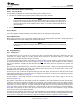


Table Of Contents
- 1 Features
- 2 Description
- Table of Contents
- 3 Revision History
- 4 Description (Continued)
- 5 Pin Configuration and Functions
- 6 Specifications
- 7 Parameter Measurement Information
- 8 Detailed Description
- 9 Application And Implementation
- 10 Power Supply Recommendations
- 11 Device and Documentation Support
- 12 Mechanical, Packaging, and Orderable Information

22
I/O
Port
P17−P10
Shift
Register
16 Bits
LP Filter
Interrupt
Logic
Input
Filter
23
Power-On
Reset
Read Pulse
Write Pulse
PCA9539
3
2
21
1
24
12
GND
V
CC
SDA
SCL
A1
A0
INT
I
2
C Bus
Control
P07−P00
RESET
PCA9539
SCPS130G –AUGUST 2005–REVISED JUNE 2014
www.ti.com
8 Detailed Description
8.1 Functional Block Diagram
A. Pin numbers shown are for DB, DBQ, DGV, DW, and PW packages.
B. All I/Os are set to inputs at reset.
Figure 17. Logic Diagram (Positive Logic)
14 Submit Documentation Feedback Copyright © 2005–2014, Texas Instruments Incorporated
Product Folder Links: PCA9539