
User's Manual
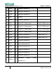
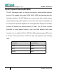
Table Of Contents

SKYLAB M&C Technology Co., Ltd SKB360 -Datasheet
8
SKB360 -DA-001,A/2
25
SWDIO/
nRESET
Hardware debug ;Flash
program I/O;
System reset (active low)
Interfaces Configuration
Power Supply
Regulated power for the SKB360I is required. The input voltage Vcc should be
1.8V to 3.6V range, current is no less than 50mA. Suitable decoupling must be
provided by external decoupling circuitry (10uF and 1uF). It can reduce the Noise
from power supply and increase power stability.
Flash program I/Os
The module has two programmer pins, respectively SWCLK pin and SWDIO
pin. The two pin Serial Wire Debug (SWD) interface provided as a part of the De
bug Access Port (DAP) offers a flexible and powerful mechanism for non-intrusiv
e debugging of program code. Breakpoints and single stepping are part of this
support.
SWDIO can also be use as system reset pin,the system reset pin is avtive low.
GPIO
The general purpose I/O is organized as one port with up to 20 I/Os enabling
access and control of up to 20 pins through one port. Each GPIO can be access
ed individually with the following user configurable features: