
User Manual

SGD-SB2025NT-TUM, Part 1
Jan 12 Page 28 GENERAL DESCRIPTION
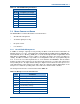
The environment I/O is arranged into two groups where each group connects to the same physical
device (integrated circuit). To keep the power dissipation of each device within operating limits, the
total current that may be switched by all the control outputs in one group must not exceed 500 mA
when all outputs are “ON”.
4.3 M
ODULE
F
UNCTIONAL
D
ESCRIPTION
4.3.1 Exciter Module
The Exciter module generates the low level, on frequency, RF Tx signal that is later amplified to
nominal output power level by the PA module. The Exciter consists of a VCO and associated main
RF board, which, in conjunction with the reference oscillator and the PLL circuitry, forms a two-
point modulation programmable frequency synthesiser. Frequency programming data is received
from the Micro Controller via a 3-wire serial data bus.
The Exciter module features a modulation bandwidth from DC with an ultra wide RF bandwidth of
20 MHz to 1000 MHz at an average RF output power of 300 mW. To change from one band to
another, all that is required is to change the plug-in VCO board and reprogram the radio. No other
manual adjustment or change is required.
Should a high stability reference be required, the exciter can be fitted with a connector for an
external reference oscillator input.
The fractional N synthesiser provides ultra low spurii while still maintaining fast lock times even at
6.25 kHz step size.
An optional built-in turn around mixer provides advanced diagnostics such as Rx sensitivity tests.
4.3.2 Receiver Module
The Rx module accepts the low level RF input signal and amplifies, filters and conditions the signal
prior to detecting the wanted audio component. The Rx module features the same advanced
synthesiser and wide bandwidth as the Exciter. Only the front-end bandpass filter and VCO need
to be changed in order to support different frequency bands, resulting in significant flexibility and
end-user cost savings. The purpose built front-end bandpass filter has a wide no-adjust bandwidth
equal to the band allocation (refer to Appendix A for details of the band allocations).
The Rx has high sensitivity while maintaining excellent intermodulation immunity and adjacent
channel rejection. A dual first Intermediate Frequency (IF) filter provides excellent rejection to
common known spurious responses. High blocking of over 100 dB typical ensures that strong
interfering signals do not desensitise the Rx when receiving weak signals.
4.3.3 Power Amplifier Module
RF from the Exciter passes via a coaxial cable to the input of the PA Module and is first attenuated
by a 50 Ω pad, which is used to provide a good 50 Ω source impedance for the first Laterally
Diffused Metal Oxide Semiconductor (LDMOS) driver amplifier. The RF is amplified to around
5 Watts at the driver output, and is band dependant. (Note. This point does not have 50 Ω
impedance and the drive power cannot be measured directly with a 50 Ω Wattmeter). The signal
from the driver is then matched by a broadband network to drive the low input impedance
associated with the final transmit LDMOS PA transistor. The transistor’s low drain impedance is
then also matched back to 50 Ω by a broadband matching network covering a very wide
bandwidth. Prior to transmission, a low loss 13 element elliptical low pass filter, filters out the
unwanted harmonics to less than –90 dBc.
A dual directional coupler consists of coupled microstrip transmission lines fabricated on the PCB
artwork. The sampled RF energy is rectified to provide a proportional DC voltage output.