
User Manual

SGD-SB2025NT-TUM, Part 1
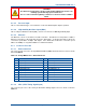
Jan 12 Page 31 TECHNICAL DESCRIPTION
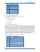
5 TECHNICAL DESCRIPTION
The internal design of the SB2025NT is of a modular nature allowing for simple configuration and
maintenance while ensuring minimal downtime. For reference purposes, the block diagram of the
SB2025NT is shown in Figure 4.
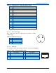
5.1 E
XCITER
M
ODULE
RF from the VCO on SKU-1 at a nominal level of +3 dBm is applied to the fractional-N synthesiser
IC10 main divider input. This signal is compared with the reference oscillator frequency and the
correction voltage from the synthesiser’s charge pump output is filtered then amplified by the non-
inverting low noise operational amplifier IC9A. This correction voltage is fed back to the VCO to
maintain loop lock, as well as being fed to the Micro Controller via SKD-14. A lock detect signal
from IC10 is also fed to the Micro Controller via SKD-16. The operational amplifier uses a 25 V
power supply (generated on the Micro Controller) in order to provide a wide tuning range voltage to
the frequency control varicaps located on the VCO board. Frequency programming data for the
Exciter is sent to the synthesiser chip from the Micro Controller via a serial data line on SKD-18
under the control of the Clock (SKD-15) and Strobe (SKD-17) lines.
Provision is made for the optional injection of an external reference frequency. If this option is
selected, CN3 is fitted and X1 is not fitted. Components R30 and TR7 are also omitted.
A second RF output from the VCO on SKT-6 also at +3 dBm is used as the main transmit RF
amplifier signal source. This main signal is first buffered by a very high isolation circuit consisting
of a 10 dB pad and a Monolithic Microwave Integrated Circuit (MMIC) amplifier (IC1). The signal is
further amplified by IC2 and a variable gain wide band amplifier with 40 dB control range and
power output of 300 mW. The drive power of this stage is used to set the output power to the main
PA under the control of the DC voltage on SKD-4 from the Micro Controller board.
The VCO boards and synthesiser circuits are the same for the Exciter and Rx modules. The VCO
consists of a 10 mm ceramic coaxial resonator with common base oscillator for low phase noise for
bands 805 MHz - 960 MHz. Frequencies below 520 MHz use a LC tank circuit. The power supply
to the VCO consists of an 8 V regulator and active filter for maximum noise rejection. It is
controlled by the Micro Controller through SKD-7, which connects to switch TR6. For standard
modulation, transmit audio is fed on SKD-8 to the conventional point of the VCO varactor. For two
point modulation, audio is also fed via SKD-19 to the voltage control pin of the VC-TXCO, this in
effect cancels out the PLL error that would otherwise have occurred for low audio frequencies,
therefore, resulting in a flat VF response.
5.2 R
ECEIVER
M
ODULE
The Rx signal from the antenna enters on CN1 a three section bandpass filter, which provides the
initial filtering for the front-end amplifier. The front-end amplifier IC12 is a broadband high
performance MMIC with a gain of 18 dB, noise figure of 3 dB and third order intermodulation
intercept of +36 dB. A 4 dB pad and a second three section bandpass filter follow this, and a high
level double balanced mixer M1.
The Rx uses high side local oscillator injection for bands A to M and low side injection for all other
bands. RF from the VCO main output on SKT-6 is buffered and amplified to +17 dBm by IC4 and
injected in the high level mixer, which down converts the signal to the first IF frequency of 90 MHz
(45 MHz for bands A and B, and 70 MHz for bands A4). This IF signal from the mixer is terminated
by a bi-directional constant impedance network and is then amplified by a bipolar amplifier TR2
with a gain of 15 dB and third order intermodulation intercept of +35 dB. This provides a high
degree of intermodulation rejection for the Rx. A 4-pole crystal filter FL3A/B with its associated
matching networks follows this stage. The signal is further amplified and filtered by a transistor
amplifier TR3 and its associated 2-pole crystal filter FL4 before being fed into the main IF
demodulator chip IC1 with a second IF frequency of 455 kHz. The resulting audio is passed out to