
hardware design v1.00
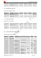

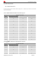


Table Of Contents
- Contents
- Version History
- 1 Introduction
- 2 SIM968 Overview
- 3 Package Information
- 4 GSM Application Interface
- 4.1 GSM Power Supply
- 4.2 Power on/down Scenarios
- 4.3 Power Saving Mode
- 4.4 Charging Interface
- 4.5 RTC Backup
- 4.6 Serial Interfaces
- 4.7 Audio Interfaces
- 4.8 SIM Card Interface
- 4.9 LCD Display/SPI Interface
- 4.10 Keypad Interface
- 4.11 ADC
- 4.12 RI Behaviors
- 4.13 Network Status Indication
- 4.14 General Purpose Input/Output (GPIO)
- 4.15 External Reset
- 4.16 PWM
- 4.17 I2C Bus
- 4.18 GSM Antenna Interface
- 5 GNSS Application Interface
- 6 Electrical, Reliability and Radio Characteristics
- 6.1 Absolute Maximum Ratings
- 6.2 Recommended Operating Conditions
- 6.3 Digital Interface Characteristics
- 6.4 SIM Card Interface Characteristics
- 6.5 VDD_EXT Characteristics
- 6.6 SIM_VDD Characteristics
- 6.7 VRTC Characteristics
- 6.8 Current Consumption (VBAT = 3.8V)
- 6.9 Electro-Static Discharge
- 6.10 Radio Characteristics
- 6.11 Module label information
- Appendix

Smart Machine Smart Decision
SIM968_Hardware Design_V1.00 2013.02.25
53
6.10 Radio Characteristics
6.10.1 Module RF Output Power
The following table shows the module conducted output power, it is followed by the 3GPP TS 05.05 technical
specification requirement.
Table 31: SIM968 GSM 900 and GSM 850 conducted RF output power
GSM 900 and EGSM 850
Tolerance (dB) for conditions
PCL Nominal output power (dBm)
Normal Extreme
0-2 39 ±2 ±2.5
3 37 ±3 ±4
4 35 ±3 ±4
5 33 ±3 ±4
6 31 ±3 ±4
7 29 ±3 ±4
8 27 ±3 ±4
9 25 ±3 ±4
10 23 ±3 ±4
11 21 ±3 ±4
12 19 ±3 ±4
13 17 ±3 ±4
14 15 ±3 ±4
15 13 ±3 ±4
16 11 ±5 ±6
17 9 ±5 ±6
18 7 ±5 ±6
19-31 5 ±5 ±6
Table 32: SIM968 DCS 1800 and PCS 1900 conducted RF output power
DCS 1800 and PCS 1900
Tolerance (dB) for conditions
PCL Nominal output power (dBm)
Normal Extreme
29 36 ±2 ±2.5
30 34 ±3 ±4
31 32 ±3 ±4
0 30 ±3 ±4
1 28 ±3 ±4
2 26 ±3 ±4