
hardware design v2.00
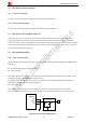
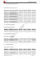
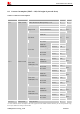
Table Of Contents
- Contents
- Version History
- 1 Introduction
- 2 SIM908 Overview
- 3 Package Information
- 4 GSM Application Interface
- 4.1 Power Supply
- 4.2 Power on/down Scenarios
- 4.3 Power Saving Mode
- 4.4 Charging Interface
- 4.5 RTC Backup
- 4.6 Serial Interfaces
- 4.7 Audio Interfaces
- 4.8 SIM Card Interface
- 4.9 LCD Display/SPI Interface
- 4.10 Keypad Interface
- 4.11 ADC
- 4.12 RI Behaviors
- 4.13 Network Status Indication
- 4.14 General Purpose Input/Output (GPIO)
- 4.15 PWM
- 4.16 I2C Bus
- 4.17 GSM Antenna Interface
- 5 GPS Application Interface
- 6 Electrical, Reliability and Radio Characteristics
- 6.1 Absolute Maximum Ratings
- 6.2 Recommended Operating Conditions
- 6.3 Digital Interface Characteristics
- 6.4 SIM Card Interface Characteristics
- 6.5 VDD_EXT Characteristics
- 6.6 SIM_VDD Characteristics
- 6.7 VRTC Characteristics
- 6.8 Current Consumption (VBAT = 3.8V, GPS engine is powered down)
- 6.9 Electro-Static Discharge
- 6.10 Radio Characteristics
- 6.11 Module label information
- Appendix

Smart Machine Smart Decision
SIM908_Hardware Design_V2.00 2012.05.07
44
product and other conditions.
For detailed Antenna designing consideration, please refer to related antenna vendor’s design recommendation.
The antenna vendor will offer further technical support and tune their antenna characteristic to achieve successful
GPS reception performance depending on the customer’s design.
6 Electrical, Reliability and Radio Characteristics
6.1 Absolute Maximum Ratings
The absolute maximum ratings stated in following table are stress ratings under non-operating conditions. Stresses
beyond any of these limits will cause permanent damage to SIM908.
Table 20: Absolute maximum ratings
Symbol Parameter Min Typ Max Unit
VBAT Power supply voltage - - 5.5 V
V
I
*
Input voltage -0.3 - 3.1 V
I
I
*
Input current - - 10 mA
I
O
*
Output current - - 10 mA
*
These parameters are for digital interface pins, such as keypad, GPIO, I
2
C, UART, LCD, PWMs and DEBUG.
6.2 Recommended Operating Conditions
Table 21: Recommended operating conditions
Symbol Parameter Min Typ Max Unit
VBAT Power supply voltage 3.2 4.0 4.8 V
T
OPER
Operating temperature -40 +25 +85 ℃
T
STG
Storage temperature -45 +90 ℃
6.3 Digital Interface Characteristics
Table 22: Digital interface characteristics
Symbol Parameter Min Typ Max Unit
I
IH
High-level input current -10 - 10 uA
I
IL
Low-level input current -10 - 10 uA
V
IH
High-level input voltage 2.4 - - V
V
IL
Low-level input voltage - - 0.4 V
V
OH
High-level output voltage 2.7 - - V
V
OL
Low-level output voltage - - 0.1 V
* These parameters are for digital interface pins, such as keypad, GPIO, I
2
C, UART, LCD, PWMs and DEBUG.