
hardware design v2.00
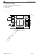
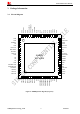
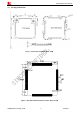
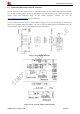
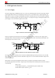
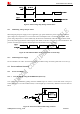
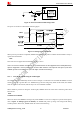
Table Of Contents
- Contents
- Version History
- 1 Introduction
- 2 SIM908 Overview
- 3 Package Information
- 4 GSM Application Interface
- 4.1 Power Supply
- 4.2 Power on/down Scenarios
- 4.3 Power Saving Mode
- 4.4 Charging Interface
- 4.5 RTC Backup
- 4.6 Serial Interfaces
- 4.7 Audio Interfaces
- 4.8 SIM Card Interface
- 4.9 LCD Display/SPI Interface
- 4.10 Keypad Interface
- 4.11 ADC
- 4.12 RI Behaviors
- 4.13 Network Status Indication
- 4.14 General Purpose Input/Output (GPIO)
- 4.15 PWM
- 4.16 I2C Bus
- 4.17 GSM Antenna Interface
- 5 GPS Application Interface
- 6 Electrical, Reliability and Radio Characteristics
- 6.1 Absolute Maximum Ratings
- 6.2 Recommended Operating Conditions
- 6.3 Digital Interface Characteristics
- 6.4 SIM Card Interface Characteristics
- 6.5 VDD_EXT Characteristics
- 6.6 SIM_VDD Characteristics
- 6.7 VRTC Characteristics
- 6.8 Current Consumption (VBAT = 3.8V, GPS engine is powered down)
- 6.9 Electro-Static Discharge
- 6.10 Radio Characteristics
- 6.11 Module label information
- Appendix

Smart Machine Smart Decision
4 GSM Application Interface
4.1 Power Supply
The power supply range of SIM908 is from 3.2V to 4.8V. The transmitting burst will cause voltage drop and the
power supply must be able to provide sufficient current up to 2A. For the VBAT input, a bypass capacitor (low
ESR) such as a 100 µF is strongly recommended; this capacitor should be placed as close as possible to SIM908
VBAT pins. The following figure is the reference design of +5V input power supply. The designed output for the
power supply is 4.1V, thus a linear regulator can be used.
GND
Figure 7: Reference circuit of the LDO power supply
If there is a high drop-out between the input and the desired output (VBAT), a DC-DC power supply will be
preferable because of its better efficiency especially with the 2A peak current in burst mode of the module. The
following figure is the reference circuit.
Figure 8: Reference circuit of the DC-DC power supply
The single 3.7V Li-ion cell battery can be connected to SIM908 VBAT pins directly. But the Ni-Cd or Ni-MH
battery must be used carefully, since their maximum voltage can rise over the absolute maximum voltage of the
module and damage it.
When battery is used, the total impedance between battery and VBAT pins should be less than 150
mΩ.
The following figure shows the VBAT voltage drop at the maximum power transmit phase, and the test condition
is as following:
VBAT=4.0V,
A VBAT bypass capacitor C
A
=100µF tantalum capacitor (ESR=0.7Ω),
Another VBAT bypass capacitor C
B
=1µF.
SIM908_Hardware Design_V2.00 2012.05.07
18