
hardware design v2.00
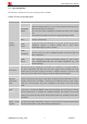
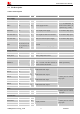
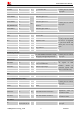
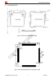
Table Of Contents
- Contents
- Version History
- 1 Introduction
- 2 SIM908 Overview
- 3 Package Information
- 4 GSM Application Interface
- 4.1 Power Supply
- 4.2 Power on/down Scenarios
- 4.3 Power Saving Mode
- 4.4 Charging Interface
- 4.5 RTC Backup
- 4.6 Serial Interfaces
- 4.7 Audio Interfaces
- 4.8 SIM Card Interface
- 4.9 LCD Display/SPI Interface
- 4.10 Keypad Interface
- 4.11 ADC
- 4.12 RI Behaviors
- 4.13 Network Status Indication
- 4.14 General Purpose Input/Output (GPIO)
- 4.15 PWM
- 4.16 I2C Bus
- 4.17 GSM Antenna Interface
- 5 GPS Application Interface
- 6 Electrical, Reliability and Radio Characteristics
- 6.1 Absolute Maximum Ratings
- 6.2 Recommended Operating Conditions
- 6.3 Digital Interface Characteristics
- 6.4 SIM Card Interface Characteristics
- 6.5 VDD_EXT Characteristics
- 6.6 SIM_VDD Characteristics
- 6.7 VRTC Characteristics
- 6.8 Current Consumption (VBAT = 3.8V, GPS engine is powered down)
- 6.9 Electro-Static Discharge
- 6.10 Radio Characteristics
- 6.11 Module label information
- Appendix

Smart Machine Smart Decision
SIM908_Hardware Design_V2.00 2012.05.07
15
I
2
C interface
I2C-SDA 56 O
I
2
C serial bus data
I2C-SCL 55 I/O
I
2
C serial bus clock
If these pins are unused,
keep open.
Keypad interface / GPIOs
GPIO1/KBR0 31 GPIO1/keypad row 0
GPIO2/KBR1 32 GPIO2/keypad row 1
GPIO3/KBR2 33 GPIO3/keypad row 2
GPIO4/KBC0/
SIM_PRESENCE
34
GPIO4/keypad column 0/ SIM card
detection
GPIO5/KBC1 35 GPIO5/keypad column 1
GPIO6/KBC2 36
I/O
GPIO6/keypad column 3
If these pins are unused,
keep open.
Serial port
RXD 68 I Receive data
TXD 71 O Transmit data
RTS 66 O Request to send
CTS 67 I Clear to send
DCD 70 O Data carrier detect
RI 69 O Ring indicator
DTR 72 I Data terminal ready
If only TXD and RXD
are used, it is suggested
to pull down DTR, and
others pins can be kept
open.
GPS/Debug interface
GPS/DBG-TXD 15 O
GPS/DBG-RXD 16 I
For GPS NMEA information output ,
debugging and upgrading firmware
If these pins are unused,
keep open.
SIM interface
SIM-VDD 20 O
Voltage supply for SIM card. Support
1.8V or 3V SIM card
SIM-DATA 17 I/O SIM data input/output
SIM-CLK 19 O SIM clock
SIM-RST 18 O SIM reset
All signals of SIM
interface should be
protected against ESD
with a TVS diode array.
ADC
ADC 47 I Input voltage range: 0V ~ 2.8V If it is unused, keep open.
Pulse width modulation( PWM )
PWM1 48 O PWM
PWM2 49 O PWM
PWM3 50 O PWM
If these pins are unused,
keep open.
GSM/GPS RF interface
GSM-ANT 59 I/O GSM radio antenna connection
Impendence must be
controlled to 50Ω.
GPS-ANT 79 I GPS radio antenna connection
Impendence must be
controlled to 50Ω.
Not connect
NC
4,11,12,13,29,30,
38,39,45,46,53,54
-
These pins should be
kept open.