
Sim800 hardware design v1.05
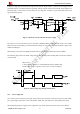
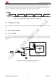
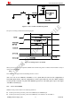
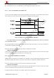
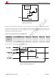
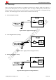
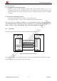
Table Of Contents
- Version History
- 1. Introduction
- 2. SIM800 Overview
- 3. Package Information
- 4. Application Interface
- 4.1. Power Supply
- 4.2. Power on/down SIM800
- 4.3. Power Saving Mode
- 4.4. RTC Backup
- 4.5. Serial Port and USB Interface
- 4.6. RI Behaviors
- 4.7. Audio Interfaces
- 4.8. Bluetooth
- 4.9. SIM Card Interface
- 4.10. PCM Interface
- 4.11. Keypad Interface
- 4.12. I2C BUS
- 4.13. General Purpose Input/Output (GPIO)
- 4.14. ADC
- 4.15. PWM
- 4.16. Network Status Indication
- 4.17. Operating Status Indication
- 4.18. KPLED
- 4.19. RF Synchronization Signal
- 4.20. Antenna Interface
- 5. PCB Layout
- 6. Electrical, Reliability and Radio Characteristics
- 6.1 Absolute Maximum Ratings
- 6.2 Recommended Operating Conditions
- 6.3 Digital Interface Characteristics
- 6.4 SIM Card Interface Characteristics
- 6.5 SIM_VDD Characteristics
- 6.6 VDD_EXT Characteristics
- 6.7 VRTC Characteristics
- 6.8 Current Consumption (VBAT=4V)
- 6.9 Electro-Static Discharge
- 6.10 Radio Characteristics
- 6.11 Module RF Receive Sensitivity
- 6.12 Module Operating Frequencies
- 7. Manufacturing
- 8. Appendix

Smart Machine Smart Decision
Figure 14: Reset circuit
The typical value of RESET pin high level is 2.8V, so for the 3V or 3.3V, customer could use MCU’s GPIO to
driver this pin directly, resistor in serial the RESET signal could enhance the ESD performance but the value
should not be too high, otherwise the level of RESET could be lower than threshold value; RESET hardware
parameters can refer to the following table.
Table 6: Electronic characteristic of the RESET Pin
Pin name Symbol Min Typ Max Unit
V
IH
2.7 2.8 2.9 V
V
IL
- - 0.6 V
RESET
T
pull down
105 - mS
The reset scenarios are illustrated in the following figures.
Figure 15: Reset timing sequence
SIM800_Hardware Design_V1.05 26 2014-03-25