
Sim800 hardware design v1.05
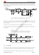
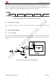
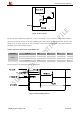
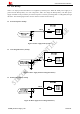
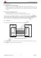
Table Of Contents
- Version History
- 1. Introduction
- 2. SIM800 Overview
- 3. Package Information
- 4. Application Interface
- 4.1. Power Supply
- 4.2. Power on/down SIM800
- 4.3. Power Saving Mode
- 4.4. RTC Backup
- 4.5. Serial Port and USB Interface
- 4.6. RI Behaviors
- 4.7. Audio Interfaces
- 4.8. Bluetooth
- 4.9. SIM Card Interface
- 4.10. PCM Interface
- 4.11. Keypad Interface
- 4.12. I2C BUS
- 4.13. General Purpose Input/Output (GPIO)
- 4.14. ADC
- 4.15. PWM
- 4.16. Network Status Indication
- 4.17. Operating Status Indication
- 4.18. KPLED
- 4.19. RF Synchronization Signal
- 4.20. Antenna Interface
- 5. PCB Layout
- 6. Electrical, Reliability and Radio Characteristics
- 6.1 Absolute Maximum Ratings
- 6.2 Recommended Operating Conditions
- 6.3 Digital Interface Characteristics
- 6.4 SIM Card Interface Characteristics
- 6.5 SIM_VDD Characteristics
- 6.6 VDD_EXT Characteristics
- 6.7 VRTC Characteristics
- 6.8 Current Consumption (VBAT=4V)
- 6.9 Electro-Static Discharge
- 6.10 Radio Characteristics
- 6.11 Module RF Receive Sensitivity
- 6.12 Module Operating Frequencies
- 7. Manufacturing
- 8. Appendix

Smart Machine Smart Decision
If there is a high drop-out between the input and the desired output (VBAT), a DC-DC power supply will be
preferable because of its better efficiency especially with the 2A peak current in burst mode of the module. The
following figure is the reference circuit. FB101 is very important, customer can get better EMI feature with
appropriate filtering bead.
Figure 7: Reference circuit of the DC-DC power supply
The single 3.7V Li-ion cell battery can be connected to IM800 VBAT pins directly. But the Ni-Cd or Ni-MH
hen battery is used, the total impedance between battery and VBAT pins should be less than 150m.
he following figure shows the VBAT voltage drop at the maximum power transmit phase, and the test condition
VBAT=4.0V,
capacitor C
A
=100µF tantalum capacitor (ESR=0.7),
S
battery must be used carefully, since their maximum voltage can rise over the absolute maximum voltage of the
module and damage it.
W
T
is as following:
A VBAT bypass
Another VBAT bypass capacitor C
B
=1µF. (See C
A
and C
B
in figure 5)
Figure 8: VBAT voltage drop during transmit burst
.1.1. Power Supply Pin
he 3 VBAT pins are used for power input, and pin 62,63,64,65 should be connected to the power GND. VRTC
hen designing the power supply in user’s application, pay special attention to power losses. Ensure that the
4
T
pin is power supply of the RTC circuit in the module. VDD_EXT will output 2.8V when module powered up.
W
SIM800_Hardware Design_V1.05 21 2014-03-25