
Users Manual Part 2

SIM8260A_Hardware Design_V1.05
www.simcom.com 70 / 122
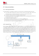
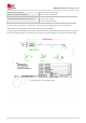
TDD_SYNC_PPS and GPS_1PPS function can’t be used at the same time.
The following is TDD_SYNC_PPS signal design guidelines:
This signal trace should be treated as a data transmission line, required impedance is 50 Ω.
This signal trace should as short as possible and cannot exceed 40mm out of the module.
This signal trace should far away from RF, power and high-speed signals.
This signal trace should be protected completely by GND.
The rising slew rate is no poor than 3ns, falling slew rate is no poor than 5ns, even with default lowest
drive strength (2mA) being selected.
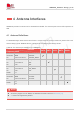
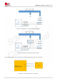
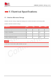
3.20 Antenna Control Interface*
ANT_CTL [0:1] and RFFE0 signals are used for tunable antenna control and should be routed to an
appropriate antenna control circuitry.
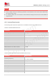
The following table are the definitions for antenna control interfaces.
Table 51: Definition of antenna control interface through GPIOs
Pin Name
Pin No.
Electrical
Description
Description
Comments
RFFE0_CLK
BA11
DO
Antenna tuner MIPI CLK
1.8V voltage
domain. If unused,
please keep open
RFFE0_DATA
BA13
DIO
Antenna tuner MIPI DATA
ANT_CTRL0
BA15
DO
Antenna tuner control0
ANT_CTRL1
AY16
DO
Antenna tuner control1
“*” means under development, for details please contact SIMCom support teams.
The RFFE0 signals are multiplexed with ANTCTL2 and ANTCTL3.
NOTE