
Users Manual Part 2

SIM8260A_Hardware Design_V1.05
www.simcom.com 51 / 122
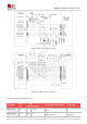
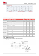
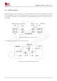
SDIO_DATA1
C1
DIO
P2
SDC data bit 1 or
eMMC data bit 1
SDIO_DATA2
D3
DIO
P2
SDC data bit 2 or
eMMC data bit 2
SDIO_DATA3
F3
DIO
P2
SDC data bit 3 or
eMMC data bit 3
SDIO_CMD
G5
DIO
P2
SDC command output
SDIO_CLK
E5
DO
P2
SDC clock output
SD_VDD_EN
H7
DO
P3
Enable the SD card power or
eMMC data bit 4
If used as eMMC
data signals,
required 45Ω
impedance
SDIO_DET
E1
DI
P3
SD card insertion detect or
eMMC data bit 5
GPIO100
H3
DIO
P3
eMMC data bit 6
GPIO101
K7
DIO
P3
eMMC data bit 7
RESOUT_N
AW17
DO
P3
eMMC RST_N
If not use SDIO interface, the SD_VDD pin should connect to VDD_EXT out of the module.
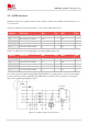
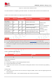
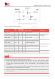
Table 29: Recommended TVS and SD card socket list
Name
Manufacturer
Model
TVS
ON
ESD9L5.0ST5G
SD card socket
ALPS
SCHA4B0400
eMMC
SanDisk
SDINBDG4_8G
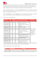
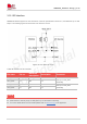
SDIO interface layout guidelines:
Require trace impedance is 45Ω.
CLK to DATA/CMD length mismatch is less than 0.5mm.
33Ω termination resistance on clock be placed in module.
Gap from other signals keeps 1.5xline width.
Gap lane-to-lane 1.5xline width.
Bus capacitance load is less than 5pF.
Trace routes away from other sensitive signals.
Maximum PCB trace length cannot exceed 30mm out of the module for 104Mbps data rate, the shorter
trace and better.
Maximum PCB trace length cannot exceed 100mm out of the module for 50Mbps data rate, the shorter
trace and better.
NOTE