
Users Manual Part 2

SIM8260A_Hardware Design_V1.05
www.simcom.com 64 / 122
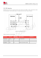
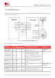
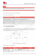
3.15 PM7250B Interface
SIM8260A supports PM7250B interface, customers can use PM7250B to manage the charge of the module.
The reference circuits as follows:
Figure 38: PM7250B interface diagram circuit
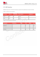
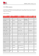
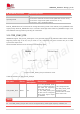
Table 44: Definition of PM7250B interface
Pin name
Pin
no.
Pin
characteristics
Functional description
Comment
USB_VBUS
C9
AI
USB VBUS detection
Not support
charge
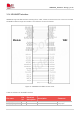
CHG_SYS_OK
C43
DI
When charger input is inserted
PM7250B output signal to PMU.
When the charging chip is not used,
this pin can be connected to GND to
realize the power-on function
FAULT_N
B44
DIO
Used to send/receive the fault
condition across all PMICs in the
chipset
SPMI_CLK
A47
DO
SPMI communication bus clock
signal
Required 50Ω
impedance
SPMI_DATA
B46
DIO
SPMI communication bus data signal
L10E_3P1
C41
PO
Output power supply for PM7250B
USB PD-PHY and USB switch
VIO_OUT
D42
PO
Output power for PM7250B IO circuit