
Users Manual Part 1

SIM8260A_Hardware Design_V1.05
www.simcom.com 39 / 122
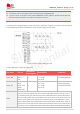
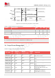
Module
state
Restar
Reseting
VBAT
Running
RESIN_N
≥
300ms
0V
≤
V
IL
≤
0.4V
1.2V
≤
V
IH
≤
1.9V
≤
600ms
T
reset
Figure 16: The reset timing sequence of the module
Table 17: RESET electronic characteristics
Symbol
Description
Min.
Typ.
Max.
Unit
T
reset
The time of holding on RESIN_N pin to a low level
300
-
600
ms
V
IH
Input high level voltage
1.2
-
1.9
V
V
IL
Input low level voltage
0
-
0.4
V
Please ensure that there is no capacitance on RESIN_N pin.
3.4 Output Power Management
Table 18: Output power management summary
Pin name
Pin
no
Typical
voltage (V)
Rated
current (mA)
Sleep
state
Comment
VDD_EXT
AL5
1.8
50
LPM
Output power supply for external
IO pull up circuits
VREG_1P3
M45
1.28
500
retention
Output power supply for W82
only
VREG_0P9
P49
0.88
1500
off
Output power supply for W82
only
VREG_1P9
N47
1.88
500
retention
Output power supply for W82
only
L10E_3P1
C41
3.08
30
off
Output power supply for
PM7250B USB PD-PHY and
USB switch
VIO_OUT
D42
1.8
0.2
on
Output power supply for
PM7250B IO circuit only
NOTE