
Users Manual Part 1

SIM8260A_Hardware Design_V1.05
www.simcom.com 27 / 122
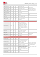
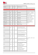
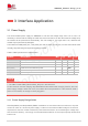
TX0/DRX_MIMO
3300MHz~5000MHz
ANT1
BA25
AI
4G/5G MHB DRX_MIMO,
5G N77/78/79 DRX
4G LAA DRX
1930MHz~2690MHz
3300MHz~5925MHz
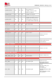
ANT2
BA33
AI
4G/5G MHB PRX_MIMO,
5G N77/78/79 PRX_MIMO,
4G LAA PRX
1930MHz~2690MHz
3300MHz~5925MHz
ANT3
BA47
AIO
4G/5G LB TX1/PRX,
5G MHB TX1/DRX,
5G N41/77/78/79 TX1/PRX
617MHz~894MHz
1710MHz~2690MHz
3300MHz~5000MHz
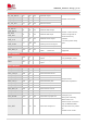
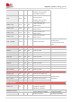
RFU PIN
RFU
BA41, AY51, BA19, B30, A29, D32, D30, D34, T45,
P45, W1
Reserved for future use
MARK
D9
PIN used inside the
module, keep it floating
externally
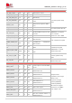
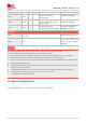
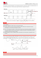
1. The I2C signals need pull up to VDD_EXT by 2.2K resistors out of the module.
2. Only used to W82 and PM7250B pins don’t use as other circuits.
3. If not use SDIO function, the SDIO_VDD pin should connect to VDD_EXT out of the module.
4. Please confirm with SIMCom for the detail design about Antenna control interface.
5. “*” means under development, for more information, please connect the SIMCom FAE support team.
RFU pins should keep open.
Recommend add ESD protect components to the interface that is touched by human hands. (e. g.
SIM/SD/USB/BUTTOM/ANT)
The GPIO MAX voltage is 2.1V, if exceeded, may cause permanent damage to the module.
All GND pins should be connected to the customer’s main PCB.
For SIM8260A module BA37 RFU.
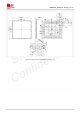
2.3 Mechanical Dimensions
The following figure shows the mechanical dimensions of SIM8260A.
NOTE