
Specifications


SIM7912&SIM7906 Hardware Design V1.02
www.simcom.com 49 / 85
If unused, keep it open.
ADC1
175
AI
Input Voltage Range:
0~1.875V
General purpose analog
to digital converter
interface
If unused, keep it open.
1. The input voltage of ADC should not exceed 1.875V
2. It is prohibited to supply any voltage to ADC pins when VBAT is removed.
3. It is recommended to use resistor divider circuit for ADC application.
3.14 GPIOs Interface
The follow pins of module can be used as GPIO function, if the customer does not use the default functions.
In addition, these pins support alternate function by software configure according to the customer’s
requirements.
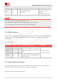
Table 29: GPIO list
Pin name
Pin no.
I/O
Functional description
Comment
GPIO_1
138
IO
General purpose input/output ports.
These four GPIOs can also be
multiplexed into a group of PCM or I2S
for BT.
1.8V power domain.
If unused, keep it open.
GPIO_2
139
IO
GPIO_3
159
IO
GPIO_4
161
IO
GPIO_5
172
IO
General purpose input/output ports.
This GPIO can also be multiplexed into
1PPS for GNSS.
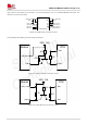
3.15 Network Status Indication
The network indication pins can be used to drive network status indication LEDs. The following tables
describe pin definition and logic level changes in different network status.
Table 30: Definition of network indication pins
NOTE