
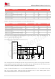
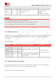
Specifications


SIM7912&SIM7906 Hardware Design V1.02
www.simcom.com 43 / 85
Pin name
Pin no.
I/O
Functional description
Comment
PCM_OUT
68
DO
PCM data output. It can also be
multiplexed as I2S_D1.
1.8V power domain.
If unused, please keep
open.
PCM_IN
66
DI
PCM data input. It can also be
multiplexed as I2S_D0.
1.8V power domain.
If unused, keep it open.
PCM_CLK
67
DO
PCM data clock. It can also be
multiplexed as I2S_CLK.
1.8V power domain.
In master mode, it is an
output signal.
In slave mode, it is an
input signal.
If unused, keep it open.
PCM_SYNC
65
DIO
PCM data frame synchronization
signal. It can also be multiplexed as
I2S_WS.
1.8V power domain.
In master mode, it is an
output signal.
In slave mode, it is an
input signal.
If unused, keep it open.
I2S_MCLK
152
DO
Clock output
Provide a digital clock
output for an external
audio codec.
If unused, keep it open.
Table 23: PCM / I2S format
For more details about PCM/I2S AT commands, please refer to Document [1] in the appendix.
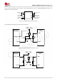
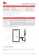
3.9.1 I2S Timing
The module supports I2S sampling rate of 48 KHz and 32bit coding signal (16bit length), the timing
sequence is shown in the following figure.
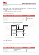
Characteristics
Specification
Line interface format
Linear(fixed)
Data length
16bits(fixed)
I2S flock/sync source
Master mode(fixed)
I2S clock rate
1.536 MHz (default)
I2S MCLK rate
12.288MHz (default)
Data ordering
MSB
NOTE