
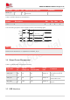
Specifications


SIM7912&SIM7906 Hardware Design V1.02
www.simcom.com 35 / 85
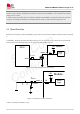
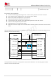
Close to Host
100nF
C1
USB_DP
USB_DM
100nF
USB_SS_TX_P
USB_SS_TX_M
USB_SS_RX_P
USB_SS_RX_M
Base
band
Module
USB_VBUS
Host
USB_SS_TX_P
USB_SS_TX_M
USB_SS_RX_P
USB_SS_RX_M
USB_DP
USB_DM
VDD
USB_ID
GPIO
GND
GND
100nF
100nF
3.6V~5.25V
C2
GPIO
Q1
R1
Choose one of
R1 and Q1
G
S
D
0Ω
Figure 15: Reference Circuit of USB Application
1. USB_VBUS is used for USB insertion detection. Its voltage input range is 3.6V~5.25V.
2. For sleep mode, if the Host does not support USB suspend mode, the input of USB_VBUS needs to
be controlled by host. Choosing Q1 for placement.
3. For sleep mode, if the host supports USB suspend mode, USB_VBUS can be directly connected to
VDD. Choosing R1 for placement.
4. The capacitors C1/C2 need to be placed close to the Host side.
5. Recommended add a 1Ω resistor in series and parallel varistor in USB3.0 for ESD protection.
HS USB DP/DM layout guidelines:
Require differential trace impedance is 90±10% Ω.
The intra-lane length mismatch of the differential signal lanes is less than 1mm.
Gap from other signals keeps 3xline width.
External components should be placed near the USB connector.
Trace routes away from other sensitive signals (RF, audio, and 38.4M XO).
Maximum PCB trace length cannot exceed 100mm outside of module, the shorter trace and more
better.
SS USB TX/RX layout guidelines:
Require differential trace impedance is 90±10% Ω.
The intra-lane length mismatch of the differential signal lanes is less than 500um.
NOTE