
Specifications


SIM7912&SIM7906 Hardware Design V1.02
www.simcom.com 33 / 85
Pin name
Pin no.
I/O
Functional description
Comment
RESET_N
1
DI
Reset the module
active low
Table 13: RESET electronic characteristics
Symbol
Description
Min.
Typ.
Max.
Unit
T
reset
The time of holding on RESET_N pin to a low level
250
500
-
ms
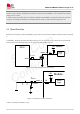
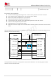
The reset timing sequence of the module is shown in the following figure.
Module
state
Restar
Reseting
VBAT
Running
RESET_N
≥500ms
0V ≤VIL ≤0.4V
1.2V ≤VIH ≤1.9V
Figure 14: The reset timing sequence of the module
Please ensure that there is no capacitance on RESET_N pin.
3.4 Output Power Management
Table 14: Output power management summary
Pin name
Pin
no
Typical
voltage (V)
Rated
current (mA)
Sleep
state
Comment
VDD_EXT
168
1.8
50
Always on
Output power supply
for external IO pull up
circuits
VDD_RF
162
2.8
150
Always on
Provide 2.85V for
external RF circuit.
SD_VDD
46
1.8/3
150
Always on
SDIO pull up power
source
3.5 USB Interface
NOTE