
Specifications


SIM7912&SIM7906 Hardware Design V1.02
www.simcom.com 27 / 85
To decrease the voltage dropping, make sure that the capacitors of VBAT net must not less than 640uF.
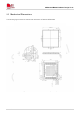
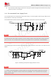
The following figure shows the reference circuit of power supply for the VBAT.
C7
100uF
C6
100nF
C8
33pF
C4
33pF
VBAT_BB
VBAT_RF
TVS1
VBAT
C1
220uF
5
V
C3
100nF
C2
C5
220uF
100uF
Module
FB101
Figure 5: Power supply reference circuit
In this reference circuit, some multi-layer ceramic chip (MLCC) capacitors (0.1/1uF) with low ESR in high
frequency band can be used for EMI suppression.
1. Both C1 and C5 are 220 µF tantalum capacitor (ESR=0.7Ω).
2. C3, C4, C7 and C8 are multi-layer ceramic chip (MLCC) capacitors from 0.1uF to 1uF with low ESR
in high frequency band, which can be used for EMC performance.
3. TVS1 is used for surge protection.
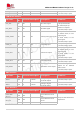
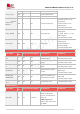
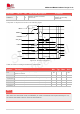
Table 8: Recommended TVS1 list
Power supply layout guidelines:
Both VBAT and return path should be as short and wide as possible to minimize the voltage drop.
The width of VBAT_BB trace should be no less than 1.5mm, and the width of VBAT_RF trace
should be no less than 2mm.
These capacitors should be placed as closely as possible to the VBAT_BB and VBAT_RF pins.
The VBAT trace should pass through TVS and capacitors, and then pass through the VBAT pins.
The small value capacitors should be placed close to the VBAT pins.
No.
Manufacturer
Part Number
Power dissipation
Package
1
Js-ele
ESDBW5V0A1
5V
DFN1006-2L
2
Prisem
PESDHC2FD4V5BH
4.5V
DFN1006-2L
3
Way-on
WS05DPF-B
5V
DFN1006-2L
4
Will semi
ESD5611N
5V
DFN1006-2L
5
Will semi
ESD56151W05
5V
SOD-323
6
Way-on
WS4.5DPV
4.5V
DFN1610-2L
NOTE