
Specifications


SIM7912&SIM7906 Hardware Design V1.02
www.simcom.com 40 / 85
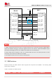
Require trace impedance is 36 to 50Ω.
CLK to DATA/CMD length mismatch is less than 0.5mm.
30–35Ω termination resistance on clock net and placed close to the module.
Gap from other signals keeps 1.5xline width.
Gap lane-to-lane 1.5xline width.
Bus capacitance load is less than 5pF.
Trace routes away from other sensitive signals.
Maximum PCB trace length cannot exceed 30mm out of the module for 104Mbps data rate, the
shorter trace and more better.
Maximum PCB trace length cannot exceed 100mm out of the module for 50Mbps data rate, the
shorter trace and more better.
It is recommended to keep the trace length difference between CLK and DATA/CMD less than
1mm and the total routing length less than 100mm. The total trace length inside the module is
25mm, so the exterior total trace length should be less than 75mm.
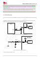
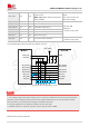
3.8 SIM Interface
Module supports two SIM cards but single standby. SIM1 and SIM2 are dual-voltage 1.8 V or 3.0 V
interfaces.
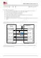
Table 18: Definition of SIM interface
Pin name
Pin no.
I/O
Functional description
Comment
SIM1_VDD
26
PO
Power supply for SIM1 card
1.8/3.0V voltage domain,
SIM interface should be
protected against ESD.
If unused, please keep
open
SIM1_DATA
29
DIO
SIM1 card data signal, which has been
pulled up to SIM1_VDD by a 20K
resistor internally
SIM1_CLK
27
DO
SIM1 clock signal
SIM1_RST
28
DO
SIM1 reset signal
SIM1_DET
25
DI
SIM1 card detect signal, which need
pulled up to VDD_EXT by a 470K
resistor externally
SIM2_VDD
74
PO
Power supply for SIM2 card
SIM2_DATA
77
DIO
SIM2 card data, which has been pulled
up to SIM2_VDD by a 20K resistor
internally
SIM2_CLK
80
DO
SIM2 clock signal
SIM2_RST
79
DO
SIM2 reset signal
SIM2_DET
78
DI
SIM2 card detect, which need pulled
up to VDD_EXT by a 470KR resistor
externally
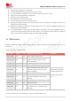
Table 19: SIM electronic characteristics in 1.8V mode (SIM_PWR=1.8V)