
Specifications


SIM7912&SIM7906 Hardware Design V1.02
www.simcom.com 37 / 85
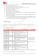
PCIe interface layout guidelines:
All other sensitive/high-speed signals and circuits must be protected from PCIe corruption.
PCIe signals must be protected from noisy signals (clocks, SMPS).
Each trace needs to be adjacent to a ground plane.
Require differential trace impedance is 90±10% Ω.
The intra-lane length mismatch of the differential signal lanes is less than 500um.
Gap from other signals keeps 4xline width.
Gap between Rx-to-Tx keeps 4xline width.
Maximum PCB trace length cannot exceed 150mm outside of module, the shorter trace and more
better.
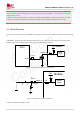
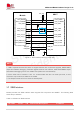
In Root Complex Mode, the module is configured to act as a PCIe RC device. The following figure shows a
reference circuit of PCIe RC mode.
Module
WLAN device
100nF
PCIe_REFCLK_M
PCIe_REFCLK_P
PCIe_ RXM
PCIe_ RXP
PCIe_ CLKM
PCIe_ CLKP
PCIe_WAKE
PCIe_RST
PCIe_CLKREQ
PCIe_TX _M
PCIe_TX _P
PCIe_RX _M
PCIe_RX _P
PCIe_ TXM
PCIe_ TXP
100nF
100nF
100nF
PCIe_RST
PCIe_WAKE
PCIe_CLKREQ
VDD_EXT
100K
100K
100K
Close to Wlan
Figure 16: PCIe interface reference circuit (RC Mode)
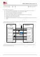
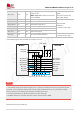
In Endpoint Mode, the module is configured to act as a PCIe EP device. The following figure shows a
reference circuit of PCIe EP mode
input signal.
If unused, keep it open