
Specifications


SIM7912&SIM7906 Hardware Design V1.02
www.simcom.com 16 / 85
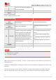
1. Keep all RESERVED pins and unused pins unconnected.
2. GND pins 215~299 should be connected to ground in the design.
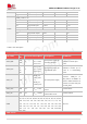
2.2 Pin Description
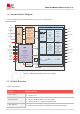
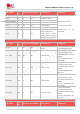
Table 4: IO parameters definition
Pin type
Description
PI
Power Input
PO
Power Output
AI
Analog Input
AIO
Analog Input /Output
DIO
Bidirectional Digital Input /Output
DI
Digital Input
DO
Digital Output
PU
Pull Up
PD
Pull Down
OD
Open Drain
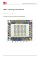
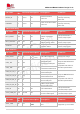
Table 5: DC parameters definition
Voltage
domain
Parameter
Min
Typ
Max
P2
VDD_P2=1.8V
V
OH
High level output
1.4V
-
-
V
OL
Low level output
0V
-
0.45V
V
IH
High level input
1.3V
-
2V
V
IL
Low level input
0.3V
-
0.58V
VDD_P2=3.0V
V
OH
High level output
2.15V
-
-
V
OL
Low level output
0V
-
0.35V
V
IH
High level input
1.8V
-
3.15V
V
IL
Low level input
0.3V
-
0.7V
P3
VDD_P3=1.8V
V
OH
High level output
1.35V
-
1.8V
V
OL
Low level output
0V
-
0.45V
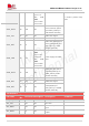
NOTE