
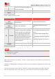
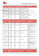
Specifications


SIM7912&SIM7906 Hardware Design V1.02
www.simcom.com 12 / 85
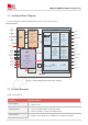
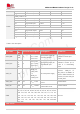
1.2 Hardware Block Diagram
The block diagram of SIM7912&SIM7906 is shown in the following figure.
ANT MAIN
Memory
Support
EBI1
Internal memory
EBI2
Internal
functions
Resource and pwr
mgt
Security and QFP
ROM
GP clock and PDM
outs
JTAG
Modes, resets, config
Clock generation
GPIOs
Processors
Cortex-A7
Hexagon DSP:
Modem
Audio
RPM cortex-M3
Air interfaces
WCDMA
processing
LTE processing
GSM processing
Qualcomm
Location
Suite; Gen 9V1
Chipset and
RFFE I/Fs
Serial interfaces
Qlink digital
interface
Connectivity
PCEe UART PCM
(audio*2) SPI I2S
I2C UIM1/UIM2(dual-V) USB2.0/USB3.0
Secure digital 3.0(dual-V)
Baseband
PMIC
Input pwr mgt
Out pwr mgt
User I/Fs
General housekeeping
IC-level I/Fs
MEMORY
NAND+LPDDR2
Transceiver
SDR modem subsystem
(SDR MSS)
RF transmitters for dual
UL
(Tx0/Tx1)
RF receivers with carrier
aggregation support
GNSS
MODULE
ANT DIV
ANT MIMO1
ANT MIMO2
ANT GNSS
RESET_N
PWRKEY
BT_EN
WLAN_PWR_EN
SIM1 Card
SIM2 Card
USB2.0/USB3.0
I2C
SD Card
UART
PCM
RFFE_CLK/DATA
USB_BOOT
PCIe
GPIOs
SD_VDD
VDD_RF
VDD_EXT
VDD_P2
VBAT_BB
VBAT_RF
ADC(*2)
WLAN_SLP_CLK
I2S_MCLK
Tx/Rx
Bolcks
PRx
DRx
MIMO
Tx
QLINK
Control
Control
38.4M
XO
Figure 1: SIM7912&SIM7906 module block diagram
1.3 Feature Overview
Table 3: Key features
Feature
Implementation
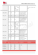
Power supply
VBAT:3.3V~4.3V
Typical: 3.8V
Transmit power
Class 3 (23dBm±2dB) for LTE-TDD bands
Class 3 (23dBm±2dB) for LTE-FDD bands
Class 3 (24dBm+1/-3dB) for WCDMA bands
LTE Features
Support FDD/TDD LTE Category 12 with CA and MIMO
Support uplink QPSK and 16-QAM and **64-QAM modulation