
Specifications

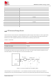

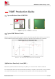
Table Of Contents
- 1Introduction
- 1.1Product Outline
- 1.2Hardware Interface Overview
- 1.3Hardware Block Diagram
- 1.4Functional Overview
- 2Package Information
- 2.1Pin Assignment Overview
- 2.2Pin Description
- 2.3Mechanical Information
- 2.4Footprint Recommendation
- 3Interface Application
- 3.1Power Supply
- 3.3WAKEUP Description
- 3.5UART Interface
- 3.6RI signal behaviors
- 3.7ADC
- 3.8SIM Card Interface
- 3.9Network Status
- 4Operation Mode
- 4.1Operating mode
- 4.2PSM
- 4.3PSM wake up
- 5RF Specifications
- 5.1LTE RF Specifications
- 5.2LTE Antenna Design Guide
- 5.3RF Layout Design Guide
- 6Electrical Specifications
- 6.1Normal Operating Conditions
- 6.2Current Consumption
- 6.3ESD Notes
- 7SMT Production Guide
- 7.1Top and Bottom View of SIM7028
- 7.2Typical SMT Reflow Profile
- 7.4Baking
- 8Packaging
- 8.1Tray packaging
- 9Appendix

SIM7028 Hardware Design V1.00
www.simcom.com 36 / 48
Figure 19: Distance between RF trace and GND
GND around the ANT pin of RF do not make pads to ensure the integration of the ground.
5.3.2 LTE antenna and other communication system isolation notice
Efficiency of LTE main antenna in free space should be more than 40%
If WLAN supported, isolation of LTE main antenna and WLAN antenna should more than 15dB
If GNSS supported, isolation of LTE main antenna and GNSS antenna should more than 30dB
The isolation of different antennas should be decided by the manufacture. For more details, please
refer to the ANTENNA DESIGN GUIDELINES FOR DIVERSITY RECEIVER SYSTEM V1.01.pdf.
※ Note