
Specifications

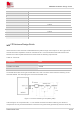
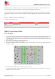
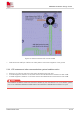
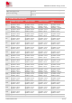

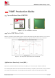
Table Of Contents
- 1Introduction
- 1.1Product Outline
- 1.2Hardware Interface Overview
- 1.3Hardware Block Diagram
- 1.4Functional Overview
- 2Package Information
- 2.1Pin Assignment Overview
- 2.2Pin Description
- 2.3Mechanical Information
- 2.4Footprint Recommendation
- 3Interface Application
- 3.1Power Supply
- 3.3WAKEUP Description
- 3.5UART Interface
- 3.6RI signal behaviors
- 3.7ADC
- 3.8SIM Card Interface
- 3.9Network Status
- 4Operation Mode
- 4.1Operating mode
- 4.2PSM
- 4.3PSM wake up
- 5RF Specifications
- 5.1LTE RF Specifications
- 5.2LTE Antenna Design Guide
- 5.3RF Layout Design Guide
- 6Electrical Specifications
- 6.1Normal Operating Conditions
- 6.2Current Consumption
- 6.3ESD Notes
- 7SMT Production Guide
- 7.1Top and Bottom View of SIM7028
- 7.2Typical SMT Reflow Profile
- 7.4Baking
- 8Packaging
- 8.1Tray packaging
- 9Appendix

SIM7028 Hardware Design V1.00
www.simcom.com 35 / 48
default, the R1, R2 are 0Ω resistors, and the C1, C2 are reserved for tuning. The component D1 is a TVS
for ESD protection, and it is optional for users according to application environment.
The RF test connector is used for the conducted RF performance test, and should be placed as close as to
the module
’
s MAIN_ANT pin. The traces impedance between SIM7028 and antenna must be controlled in
50Ω.
Two TVS are recommended in the table below.
Table 20: Recommended TVS
Package
Part Number
Vender
0201
LXES03AAA1-154
Murata
0402
LXES15AAA1-153
Murata
5.3 RF Layout Design Guide
5.3.1 RF layout
The length of RF trace between module and antenna should be as short as possible upon the antenna
position and trace loss, the module should be placed as close as possible to the main board edge.
The RF trace(micro-strip trace on top or strip trace in the inner layer) should be shielded by ground and
50Ω impedance.
RF trace should avoid right angle and acute angle.
RF trace should be shielded around GND.
RF trace examples shown in the following figure, which isolated from other high-speed signal and
shielded by GND.
Figure 18: RF trace should be isolated from other signal trace
Do not trace RF signal across or parallel with other signals
If the interface of RF is SMA, GND should has some distance away from RF pads. Do not lay the
copper in all the layers on PCB