
Specifications
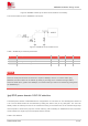
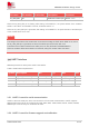
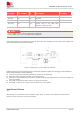
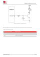
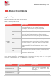
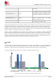
Table Of Contents
- 1Introduction
- 1.1Product Outline
- 1.2Hardware Interface Overview
- 1.3Hardware Block Diagram
- 1.4Functional Overview
- 2Package Information
- 2.1Pin Assignment Overview
- 2.2Pin Description
- 2.3Mechanical Information
- 2.4Footprint Recommendation
- 3Interface Application
- 3.1Power Supply
- 3.3WAKEUP Description
- 3.5UART Interface
- 3.6RI signal behaviors
- 3.7ADC
- 3.8SIM Card Interface
- 3.9Network Status
- 4Operation Mode
- 4.1Operating mode
- 4.2PSM
- 4.3PSM wake up
- 5RF Specifications
- 5.1LTE RF Specifications
- 5.2LTE Antenna Design Guide
- 5.3RF Layout Design Guide
- 6Electrical Specifications
- 6.1Normal Operating Conditions
- 6.2Current Consumption
- 6.3ESD Notes
- 7SMT Production Guide
- 7.1Top and Bottom View of SIM7028
- 7.2Typical SMT Reflow Profile
- 7.4Baking
- 8Packaging
- 8.1Tray packaging
- 9Appendix

SIM7028 Hardware Design V1.00
www.simcom.com 25 / 48
down as the module goes to sleep, which cannot be awake by AT command through the serial port,
only can be awake by WAKEUP pin. The external LDO as the power supply is recommended.
3.6 RI signal behaviors
RI always keep at the high level, when SMS received or URC outputs, the module will inform DTE
through RI pin.
Figure 13: RI signal behaviors(SMS, URC)
For details of this AT command, please refer to document [1].
3.7 ADC
SIM7028 provides one ADC, the electrical characteristics shown as below:
Table 10: ADC electrical characteristics
Characteristics
Min
Typ
Max
Unit
ADC resolution
–
12
–
bits
Voltage range
0
–
3.3
V
Customer can use AT command “AT+CADC?” to read the voltage value. For details of this AT
command, please refer to document [1].
3.8 SIM Card Interface
SIM7028 supports 1.8V and 3.0V SIM card. The power supply of SIM card provides by the internal
LDO.
Table 11: SIM card pin definition
※ Note
※
Note