
Specifications
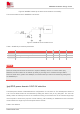
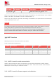
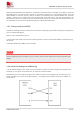
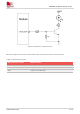
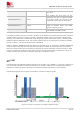
Table Of Contents
- 1Introduction
- 1.1Product Outline
- 1.2Hardware Interface Overview
- 1.3Hardware Block Diagram
- 1.4Functional Overview
- 2Package Information
- 2.1Pin Assignment Overview
- 2.2Pin Description
- 2.3Mechanical Information
- 2.4Footprint Recommendation
- 3Interface Application
- 3.1Power Supply
- 3.3WAKEUP Description
- 3.5UART Interface
- 3.6RI signal behaviors
- 3.7ADC
- 3.8SIM Card Interface
- 3.9Network Status
- 4Operation Mode
- 4.1Operating mode
- 4.2PSM
- 4.3PSM wake up
- 5RF Specifications
- 5.1LTE RF Specifications
- 5.2LTE Antenna Design Guide
- 5.3RF Layout Design Guide
- 6Electrical Specifications
- 6.1Normal Operating Conditions
- 6.2Current Consumption
- 6.3ESD Notes
- 7SMT Production Guide
- 7.1Top and Bottom View of SIM7028
- 7.2Typical SMT Reflow Profile
- 7.4Baking
- 8Packaging
- 8.1Tray packaging
- 9Appendix

SIM7028 Hardware Design V1.00
www.simcom.com 24 / 48
Figure 10: Connection of serial port with level matching
When serial port of MCU does not match the serial port of the module, the voltage level translator circuit is
recommended between them to let the voltage level match.
The following figure is the reference design circuit with translator IC:
Figure 11: The recommended circuit with the translator IC
The second level translator circuit as shown in the figure below:
Figure 12: The recommended circuit with MOSFET
Using pin of IO_1833_SEL to configure the power domain of serial port is recommended to match
the serial port of MCU to simplify the hardware design and to have the optimum cost.
The pin of VDD_EXT is not recommended as power supply of the VCC, because VCC will be shut
※
Note