
Specifications
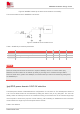
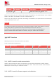
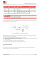
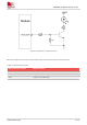
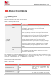
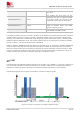
Table Of Contents
- 1Introduction
- 1.1Product Outline
- 1.2Hardware Interface Overview
- 1.3Hardware Block Diagram
- 1.4Functional Overview
- 2Package Information
- 2.1Pin Assignment Overview
- 2.2Pin Description
- 2.3Mechanical Information
- 2.4Footprint Recommendation
- 3Interface Application
- 3.1Power Supply
- 3.3WAKEUP Description
- 3.5UART Interface
- 3.6RI signal behaviors
- 3.7ADC
- 3.8SIM Card Interface
- 3.9Network Status
- 4Operation Mode
- 4.1Operating mode
- 4.2PSM
- 4.3PSM wake up
- 5RF Specifications
- 5.1LTE RF Specifications
- 5.2LTE Antenna Design Guide
- 5.3RF Layout Design Guide
- 6Electrical Specifications
- 6.1Normal Operating Conditions
- 6.2Current Consumption
- 6.3ESD Notes
- 7SMT Production Guide
- 7.1Top and Bottom View of SIM7028
- 7.2Typical SMT Reflow Profile
- 7.4Baking
- 8Packaging
- 8.1Tray packaging
- 9Appendix

SIM7028 Hardware Design V1.00
www.simcom.com 21 / 48
Figure 8: WAKEUP wakes up the serial communication successfully
The recommended circuit for WAKEUP is as follows:
Figure 9: WAKEUP recommended circuit
Table 7: WAKEUP pin electrical parameters
Symbol
Description
Min.
Typ.
Max.
Unit
T
The active low level time impulse
500
-
–
ms
VIH
Input high level voltage
1.1
1.3
1.4
V
VIL
Input low level voltage
-
-
0.3
V
When the serial port baud rate is less than or equal to 9600bps, there is no need to wake up by
WAKEUP, and the module can be waked up directly by sending an AT command through UART1.
When the baud rate is greater than 9600bps, the module wake-up needs to be realized by pulling down
the WAKEUP pin.
3.4 GPIO power domain 1.8V/3.3V selection
The GPIO power domain of SIM7028 has two configurations of 1.8V and 3.3V. The default power domain is
1.8V. The two GPIO levels can be switched by setting the state of the pin IO_1833_SEL. The user can
flexibly select the GPIO port level of the module according to the GPIO level of the external single-chip
microcomputer to achieve the purpose of level matching, without adding an additional IO level conversion
circuit between the single-chip microcomputer and the module.
Table 8: Pin definition
NOTE