
Specifications
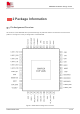
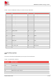
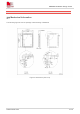
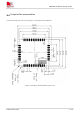
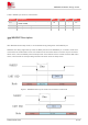
Table Of Contents
- 1Introduction
- 1.1Product Outline
- 1.2Hardware Interface Overview
- 1.3Hardware Block Diagram
- 1.4Functional Overview
- 2Package Information
- 2.1Pin Assignment Overview
- 2.2Pin Description
- 2.3Mechanical Information
- 2.4Footprint Recommendation
- 3Interface Application
- 3.1Power Supply
- 3.3WAKEUP Description
- 3.5UART Interface
- 3.6RI signal behaviors
- 3.7ADC
- 3.8SIM Card Interface
- 3.9Network Status
- 4Operation Mode
- 4.1Operating mode
- 4.2PSM
- 4.3PSM wake up
- 5RF Specifications
- 5.1LTE RF Specifications
- 5.2LTE Antenna Design Guide
- 5.3RF Layout Design Guide
- 6Electrical Specifications
- 6.1Normal Operating Conditions
- 6.2Current Consumption
- 6.3ESD Notes
- 7SMT Production Guide
- 7.1Top and Bottom View of SIM7028
- 7.2Typical SMT Reflow Profile
- 7.4Baking
- 8Packaging
- 8.1Tray packaging
- 9Appendix

SIM7028 Hardware Design V1.00
www.simcom.com 19 / 48
of 2.2V to 4.3V to the VBAT pin.
1.The voltage of VBAT must be lower than 0.7 V before power-on, and the power supply must rise to
above 2.2 V within 10 ms.
2. After VBAT is powered on, RESET automatically rises to a high level due to an internal pull-up.
3. After the VBAT voltage rises above 2.2V, the system will automatically turn on. After turning on the
VBAT voltage, the jitter cannot be lower than 2.2V, otherwise the system will be abnormal. The system
can be reset via RESET.
3.2.2 Power off
The module can be shut down by disconnecting the VBAT power supply.
3.2.3 Reset Function
SIM7028 can reset the module by keeping the RESET pin low for at least 50ms. The module can also be
reset by the AT command "AT+NRB".
The RESET signal has been pulled up inside the chip, and the RESET signal will immediately change to a
high level after the module is powered on.
Figure 6:Reference reset circuit
NOTE