
Specifications
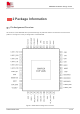
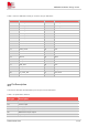
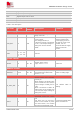
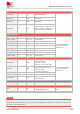
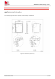
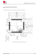
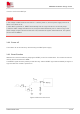
Table Of Contents
- 1Introduction
- 1.1Product Outline
- 1.2Hardware Interface Overview
- 1.3Hardware Block Diagram
- 1.4Functional Overview
- 2Package Information
- 2.1Pin Assignment Overview
- 2.2Pin Description
- 2.3Mechanical Information
- 2.4Footprint Recommendation
- 3Interface Application
- 3.1Power Supply
- 3.3WAKEUP Description
- 3.5UART Interface
- 3.6RI signal behaviors
- 3.7ADC
- 3.8SIM Card Interface
- 3.9Network Status
- 4Operation Mode
- 4.1Operating mode
- 4.2PSM
- 4.3PSM wake up
- 5RF Specifications
- 5.1LTE RF Specifications
- 5.2LTE Antenna Design Guide
- 5.3RF Layout Design Guide
- 6Electrical Specifications
- 6.1Normal Operating Conditions
- 6.2Current Consumption
- 6.3ESD Notes
- 7SMT Production Guide
- 7.1Top and Bottom View of SIM7028
- 7.2Typical SMT Reflow Profile
- 7.4Baking
- 8Packaging
- 8.1Tray packaging
- 9Appendix

SIM7028 Hardware Design V1.00
www.simcom.com 13 / 48
Table 3: Lists the SIM7028 module pin numbers and pin definitions
Pin No.
Pin Name
Pin No.
Pin Name
1
UART1_TXD
22
UART0_TXD
2
UART1_RXD
23
UART0_RXD
3
UART1_RTS
24
RESERVED
4
UART1_CTS
25
RESERVED
5
UART1_DCD
26
RESERVED
6
UART1_DTR
27
GND
7
UART1_RI
28
RESET
8
GND
29
GPIO2
9
RESERVED
30
GND
10
BOOT
31
GND
11
AON_GPIO
32
ANT
12
WAKEUP
33
GND
13
GND
34
VBAT
14
GPIO1
35
VBAT
15
SIM_DATA
36
GND
16
SIM_CLK
37
GND
17
SIM_RST
38
ADC
18
SIM_VDD
39
WAKEUP
19
GND
40
VDD_EXT
20
IO_1833_SEL
41
NETLIGHT
21
GND
42
STATUS
2.2 Pin Description
This section describes the SIM7028 of pins and pin function definitions
Table 4: IO parameters definition
Pin type
Description
PI
Power input
PO
Power output
AI
Analog input
AIO
Analog input/output
I/O
Bidirectional input /output
DI
Digital input