
Specifications
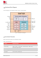
Table Of Contents
- 1Introduction
- 1.1Product Outline
- 1.2Hardware Interface Overview
- 1.3Hardware Block Diagram
- 1.4Functional Overview
- 2Package Information
- 2.1Pin Assignment Overview
- 2.2Pin Description
- 2.3Mechanical Information
- 2.4Footprint Recommendation
- 3Interface Application
- 3.1Power Supply
- 3.3WAKEUP Description
- 3.5UART Interface
- 3.6RI signal behaviors
- 3.7ADC
- 3.8SIM Card Interface
- 3.9Network Status
- 4Operation Mode
- 4.1Operating mode
- 4.2PSM
- 4.3PSM wake up
- 5RF Specifications
- 5.1LTE RF Specifications
- 5.2LTE Antenna Design Guide
- 5.3RF Layout Design Guide
- 6Electrical Specifications
- 6.1Normal Operating Conditions
- 6.2Current Consumption
- 6.3ESD Notes
- 7SMT Production Guide
- 7.1Top and Bottom View of SIM7028
- 7.2Typical SMT Reflow Profile
- 7.4Baking
- 8Packaging
- 8.1Tray packaging
- 9Appendix

SIM7028 Hardware Design V1.00
www.simcom.com 10 / 48
1.3 Hardware Block Diagram
The block diagram of the SIM7028 module is shown in the figure below.
Figure 1: SIM7028 block diagram
1.4 Functional Overview
Table 2 describes the features of the SIM7028 modules.
Table 2: General features
Feature
Implementation
Power supply
Power supply voltage:2.2V~4.3V.
Power saving
DRX:0.11mA (DRX=2.56s)
eDRX:0.018mA (PTW=25.6s;eDRX=163.84s;DRX=2.56s)
PSM mode Typical: 0.8uA
Radio frequency bands
Please refer to the table 1
Transmitting power
LTE power class: 3 (23dBm
±
2.7dB)
Data Transmission
Throughput
LTE CAT NB2: 127Kbps (DL).
LTE CAT NB2: 159Kbps (UL).
Antenna
LTE main antenna.