
Owner's manual
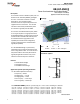

HB-HVI-5N002
Power Semiconductor Half-Bridge Module
SGTO Module
Performance Ratings
(TJ=25oC unless otherwise specified)
Parameters Symbol Min. Typ. Max. Units Test Conditions
Peak Off-State Forward Voltage(+/- or ~)
V
DRM
5 kV
Off-State rate of Change of Voltage Immunity*
dv/
dt
>
1
kV/us
I
D
50 100 uA
V
GK
=0V, V
AK
=10kV T
J
=25
o
C
100 800 uA Note: 3 & 4
T
J
=125
o
C
Peak Gate Current (1 uS)
IGpk
100 A
Gate Threshold Voltage
V
GTH
0.7 V
Gate Breakdown Voltage
V
B
10 12 TBD V
Turn-On Gate Threshold Voltage
V
GK(TH)
5
V
Continuous Anode Current at Tj = 125
o
C
I
A110
100 A
Peak Anode Current (150 uSec)
I
P at 150µs
5 KA
Peak Anode Current (1mSec)
I
P at 1ms
3 kA
R
gk
= 10 ohms V
AK
= 1500 V
Pk Rate of Change of Current (measured) dI/dt 30 kA/us
Gate di/dt =100 A/us
T
c
=25
°
C
Turn-on Delay Time
t
D(ON)
100 250 ns Ls=8.2nH
Turn-off Delay Time
t
D(OFF)
100 250 ns
C=0.15 uF Capacitor discharge
V
T
1 1.8 V
I
T
=50A T
J
=25
o
C
V Ig = 500 mA
T
J
=125
o
C
Peak Reverse Voltage
V
RRM
-10 V
Max. Reverse Gate-Cathode Voltage
V
GR
-9 V
Gate-Cathode Leakage Current
I
GK(lkg)
20 uA
V
GK
=-9V, see Note: 1
Max. Junction Temperature
T
140
°
C
Anode-Cathode Off-State Forward Leakage
Current
Anode-Cathode On-State Voltage
Max. Junction Temperature
T
JM
140
°
C
Thermal Resistance
R
JC
0.04
o
C/W
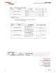
Application Note: IUT Series Resonant Inverter Stage
CAO 05/28/09
Notes:
1.) 10 Ohm shorting resistor connected between the gate and
cathode.
2. ) Case Exterior Assummed to be 0.002" of 63Sn/37Pb solder applied
directly to cathode bond area of ThinPak.
3.) Characterization accomplished using Rgk=10 ohms.
Diode Cond. loss 0.3 W
Diode Switching loss 0.2 W
Device Conduction loss 5.9 W
Device Switching loss 108 W
Module loss 229 W
2 REV 0