
User manual


...the world's most energy friendly microcontrollers
2012-04-24 - Giant Gecko Family - d0053_Rev0.96 797
www.energymicro.com
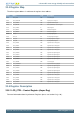
Offset Bit Position
0x000
31
30
29
28
27
26
25
24
23
22
21
20
19
18
17
16
15
14
13
12
11
10
9
8
7
6
5
4
3
2
1
0
Reset
0
0x0
0
Access
RW
RW
RW
Name
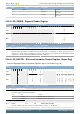
DSC
UDCTRL
EN
Bit Name Reset Access Description
31:24 Reserved
To ensure compatibility with future devices, always write bits to 0. More information in Section 2.1 (p. 3)
23 DSC 0 RW Direct Segment Control
This bit enables direct control over bias levels for each SEG/COM line.
Value Description
0 DSC disable
1 DSC enable
22:3 Reserved
To ensure compatibility with future devices, always write bits to 0. More information in Section 2.1 (p. 3)
2:1 UDCTRL 0x0 RW Update Data Control
These bits control how data from the SEGDn registers are transferred to the LCD driver.
Value Mode Description
0 REGULAR The data transfer is controlled by SW. Transfer is performed as soon as possible
1 FCEVENT The data transfer is done at the next event triggered by the Frame Counter
2 FRAMESTART The data transfer is done continously at every LCD frame start
0 EN 0 RW LCD Enable
When this bit is set, the LCD driver is enabled and the driver will start outputting waveforms on the com/segment lines.
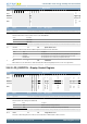
33.5.2 LCD_DISPCTRL - Display Control Register
Offset Bit Position
0x004
31
30
29
28
27
26
25
24
23
22
21
20
19
18
17
16
15
14
13
12
11
10
9
8
7
6
5
4
3
2
1
0
Reset
0
0x3
0
0
0x1F
0
0x0
0x0
Access
RW
RW
RW
RW
RW
RW
RW
RW
Name
MUXE
VBLEV
VLCDSEL
CONCONF
CONLEV
WAVE
BIAS
MUX
Bit Name Reset Access Description
31:23 Reserved
To ensure compatibility with future devices, always write bits to 0. More information in Section 2.1 (p. 3)
22 MUXE 0 RW Extended Mux Configuration
This bit redefines the meaning of the MUX field.
Value Mode Description
0 MUX Muliplex mode determined by MUX field.
1 MUXE Mux extended mode. Extends the meaning of the MUX field.
21 Reserved
To ensure compatibility with future devices, always write bits to 0. More information in Section 2.1 (p. 3)
20:18 VBLEV 0x3 RW Voltage Boost Level
These bits control Voltage Boost level. Please refer to datasheet for further details of the boost levels.