
User manual

...the world's most energy friendly microcontrollers
2012-04-24 - Giant Gecko Family - d0053_Rev0.96 723
www.energymicro.com
Bit Name Reset Access Description
2:0 POSSEL 0x0 RW OPA1 non-inverting Input Mux
These bits selects the source for the non-inverting input on OPA1
Value Mode Description
0 DISABLE Input disabled
1 DAC DAC as input
2 POSPAD POS PAD as input
3 OPA0INP OPA0 as input
4 OPATAP OPA 1 Resistor ladder as input
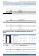
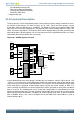
29.5.18 DACn_OPA2MUX - Operational Amplifier Mux Configuration
Register
Offset Bit Position
0x064
31
30
29
28
27
26
25
24
23
22
21
20
19
18
17
16
15
14
13
12
11
10
9
8
7
6
5
4
3
2
1
0
Reset
0x0
0
0
0x0
0
0
0x0
0x0
0x0
Access
RW
RW
RW
RW
RW
RW
RW
RW
RW
Name
RESSEL
NEXTOUT
OUTMODE
OUTPEN
NPEN
PPEN
RESINMUX
NEGSEL
POSSEL
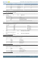
Bit Name Reset Access Description
31 Reserved
To ensure compatibility with future devices, always write bits to 0. More information in Section 2.1 (p. 3)
30:28 RESSEL 0x0 RW OPA2 Resistor Ladder Select
Configures the resistor ladder tap for OPA2.
Value Mode Resistor Value Inverting Mode Gain (-R2/R1) Non-inverting Mode Gain (1+(R2/
R1)
0 RES0 R2 = 1/3 x R1 -1/3 1 1/3
1 RES1 R2 = R1 -1 2
2 RES2 R2 = 1 2/3 x R1 -1 2/3 2 2/3
3 RES3 R2 = 2 x R1 -2 1/5 3 1/5
4 RES4 R2 = 3 x R1 -3 4
5 RES5 R2 = 4 1/3 x R1 -4 1/3 5 1/3
6 RES6 R2 = 7 x R1 -7 8
7 RES7 R2 = 15 x R1 -15 16
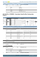
27 Reserved
To ensure compatibility with future devices, always write bits to 0. More information in Section 2.1 (p. 3)
26 NEXTOUT 0 RW OPA2 Next Enable
OPA2 does not have an next output.
25:23 Reserved
To ensure compatibility with future devices, always write bits to 0. More information in Section 2.1 (p. 3)
22 OUTMODE 0 RW Output Select
Enables opa2 main output.
21:16 Reserved
To ensure compatibility with future devices, always write bits to 0. More information in Section 2.1 (p. 3)
15:14 OUTPEN 0x0 RW OPA2 Output Location
Select location for main output
Value Mode Description
1 OUT0 Main Output 0
2 OUT1 Main Output 1
13 NPEN 0 RW OPA2 Negative Pad Input Enable