
User manual

...the world's most energy friendly microcontrollers
2012-04-24 - Giant Gecko Family - d0053_Rev0.96 717
www.energymicro.com
Bit Name Reset Access Description
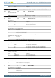
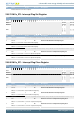
27:16 CH1DATA 0x000 W Channel 1 Data
Data written to this register will be written to DATA in DACn_CH1DATA.
15:12 Reserved
To ensure compatibility with future devices, always write bits to 0. More information in Section 2.1 (p. 3)
11:0 CH0DATA 0x000 W Channel 0 Data
Data written to this register will be written to DATA in DACn_CH0DATA.
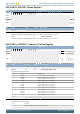
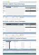
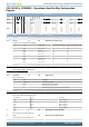
29.5.12 DACn_CAL - Calibration Register
Offset Bit Position
0x02C
31
30
29
28
27
26
25
24
23
22
21
20
19
18
17
16
15
14
13
12
11
10
9
8
7
6
5
4
3
2
1
0
Reset
0x40
0x00
0x00
Access
RW
RW
RW
Name
GAIN
CH1OFFSET
CH0OFFSET
Bit Name Reset Access Description
31:23 Reserved
To ensure compatibility with future devices, always write bits to 0. More information in Section 2.1 (p. 3)
22:16 GAIN 0x40 RW Gain Calibration Value
This register contains the gain calibration value. This field is set to the production gain calibration value for the 1V25 internal reference
during reset, hence the reset value might differ from device to device. The field is unsigned. Higher values lead to lower DAC results.
15:14 Reserved
To ensure compatibility with future devices, always write bits to 0. More information in Section 2.1 (p. 3)
13:8 CH1OFFSET 0x00 RW Channel 1 Offset Calibration Value
This register contains the offset calibration value used with channel 1 conversions. This field is set to the production channel 1 offset
calibration value for the 1V25 internal reference during reset, hence the reset value might differ from device to device. The field is
sign-magnitude encoded. Higher values lead to lower DAC results.
7:6 Reserved
To ensure compatibility with future devices, always write bits to 0. More information in Section 2.1 (p. 3)
5:0 CH0OFFSET 0x00 RW Channel 0 Offset Calibration Value
This register contains the offset calibration value used with channel 0 conversions. This field is set to the production channel 0 offset
calibration value for the 1V25 internal reference during reset, hence the reset value might differ from device to device. The field is
sign-magnitude encoded. Higher values lead to lower DAC results.
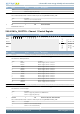
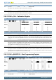
29.5.13 DACn_BIASPROG - Bias Programming Register
Offset Bit Position
0x030
31
30
29
28
27
26
25
24
23
22
21
20
19
18
17
16
15
14
13
12
11
10
9
8
7
6
5
4
3
2
1
0
Reset
1
0x7
1
0x7
Access
RW
RW
RW
RW
Name
OPA2HALFBIAS
OPA2BIASPROG
HALFBIAS
BIASPROG
Bit Name Reset Access Description
31:15 Reserved
To ensure compatibility with future devices, always write bits to 0. More information in Section 2.1 (p. 3)
14 OPA2HALFBIAS 1 RW Half Bias Current