
User manual

...the world's most energy friendly microcontrollers
2012-04-24 - Giant Gecko Family - d0053_Rev0.96 684
www.energymicro.com
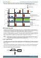
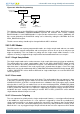
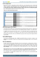
Figure 28.3. ADC Analog Power Consumption With Different WARMUPMODE Settings
ADC enabled Conversion trigger Conversion trigger
Power
Power
Power
Time
Time
ADC warm-up
ADC conversion
Bandgap reference warm -up
5 µs
1 µs 1 µs
5 µs5 µs
5 µs
NORMAL
KEEPSCANREFW ARM
(w SCANREF = internal bandgap)
KEEPADCW ARM
(w SCANREF = internal bandgap)
Power
Time
FASTBG
(w SCANREF = any)
or
NORMAL
(w SCANREF = external or VDD)
a)
b)
c)
d)
28.3.4 Input Selection
The ADC is connected to 8 external input pins, which can be selected as 8 different single ended inputs or
4 differential inputs. In addition, 6 single ended internal inputs can be selected. The available selections
are given in the register description for ADCn_SINGLECTRL and ADCn_SCANCTRL.
For offset calibration purposes it is possible to internally short the differential ADC inputs and thereby
measure a 0 V differential. Differential 0 V is selected by writing the DIFF bit to 1 and INPUTSEL to 4 in
ADCn_SINGLECTRL. Calibration is described in detail in Section 28.3.10 (p. 689) .
Note
When VDD/3 is sampled, the acquisition time should be above a lower limit. The reader is
referred to the datasheet for minimum VDD/3 acquisition time.
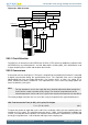
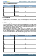
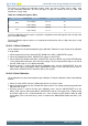
28.3.4.1 Input Filtering
The selected input signal can be filtered, either through an internal low pass RC filter or an internal
decoupling capacitor. The different filter configurations can be enabled through the LPFMODE bits in
ADCn_CTRL.
The RC input filter configuration is given in Figure 28.4 (p. 684) . The resistance and capacitance values
are given in the electrical characteristics for the device, named R
ADCFILT
and C
ADCFILT
respectively.
Figure 28.4. ADC RC Input Filter Configuration
ADC
Input
R
C