
User manual

...the world's most energy friendly microcontrollers
2012-04-24 - Giant Gecko Family - d0053_Rev0.96 635
www.energymicro.com
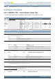
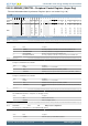
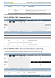
25.5.3 LESENSE_PERCTRL - Peripheral Control Register (Async Reg)
For more information about Asynchronous Registers please see Section 5.3 (p. 20) .
Offset Bit Position
0x008
31
30
29
28
27
26
25
24
23
22
21
20
19
18
17
16
15
14
13
12
11
10
9
8
7
6
5
4
3
2
1
0
Reset
0x0
0x0
0x0
0
0x00
0x0
0x0
0x0
0x0
0
0
Access
RW
RW
RW
RW
RW
RW
RW
RW
RW
RW
RW
Name
WARMUPMODE
ACMP1MODE
ACMP0MODE
DACREF
DACPRESC
DACCH1OUT
DACCH0OUT
DACCH1CONV
DACCH0CONV
DACCH1DATA
DACCH0DATA
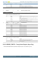
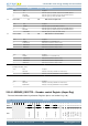
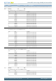
Bit Name Reset Access Description
31:28 Reserved
To ensure compatibility with future devices, always write bits to 0. More information in Section 2.1 (p. 3)
27:26 WARMUPMODE 0x0 RW ACMP and DAC duty cycle mode
Value Mode Description
0 NORMAL The analog comparators and DAC are shut down when LESENSE is idle
1 KEEPACMPWARM The analog comparators are kept powered up when LESENSE is idle
2 KEEPDACWARM The DAC is kept powered up when LESENSE is idle
3 KEEPACMPDACWARM The analog comparators and DAC are kept powered up when LESENSE is idle
25:24 Reserved
To ensure compatibility with future devices, always write bits to 0. More information in Section 2.1 (p. 3)
23:22 ACMP1MODE 0x0 RW ACMP1 mode
Configure how LESENSE controls ACMP1
Value Mode Description
0 DISABLE LESENSE does not control ACMP1
1 MUX LESENSE controls the input mux (POSSEL) of ACMP1
2 MUXTHRES LESENSE controls the input mux and the threshold value (VDDLEVEL) of ACMP1
21:20 ACMP0MODE 0x0 RW ACMP0 mode
Configure how LESENSE controls ACMP0
Value Mode Description
0 DISABLE LESENSE does not control ACMP0
1 MUX LESENSE controls the input mux (POSSEL) of ACMP0
2 MUXTHRES LESENSE controls the input mux (POSSEL) and the threshold value (VDDLEVEL) of
ACMP0
19 Reserved
To ensure compatibility with future devices, always write bits to 0. More information in Section 2.1 (p. 3)
18 DACREF 0 RW DAC bandgap reference used
Set to BANDGAP if the DAC is configured to use bandgap reference
Value Mode Description
0 VDD DAC uses VDD reference
1 BANDGAP DAC uses bandgap reference
17:15 Reserved
To ensure compatibility with future devices, always write bits to 0. More information in Section 2.1 (p. 3)
14:10 DACPRESC 0x00 RW DAC prescaler configuration.
Prescaling factor of DACPRESC+1 for the LESENSE DAC interface
9:8 DACCH1OUT 0x0 RW DAC channel 1 output mode
Value Mode Description
0 DISABLE DAC CH1 output to pin and ACMP/ADC disabled