
User manual


...the world's most energy friendly microcontrollers
2012-04-24 - Giant Gecko Family - d0053_Rev0.96 414
www.energymicro.com
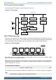
16.3 Functional Description
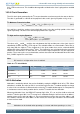
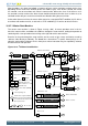
An overview of the I
2
C module is shown in Figure 16.1 (p. 414) .
Figure 16.1. I
2
C Overview
Transm it Buffer
Transm it
Shift Register
I2Cn_SDA
Receive Buffer
Receive
Shift Register
I
2
C Control and
Status
Peripheral Bus
I2Cn_SCL
Pin
ctrl
Symbol
Generator
Receive
Controller
Clock generator
Address
Recognizer
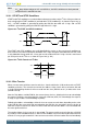
16.3.1 I
2
C-Bus Overview
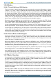
The I
2
C-bus uses two wires for communication; a serial data line (SDA) and a serial clock line (SCL) as
shown in Figure 16.2 (p. 414) . As a true multi-master bus it includes collision detection and arbitration
to resolve situations where multiple masters transmit data at the same time without data loss.
Figure 16.2. I
2
C-Bus Example
I
2
C m aster
# 1
I
2
C m aster
# 2
I
2
C slave
# 1
I
2
C slave
# 2
I
2
C slave
# 3
SDA
SCL
V
DD
R
p
Each device on the bus is addressable by a unique address, and an I
2
C master can address all the
devices on the bus, including other masters.
Both the bus lines are open-drain. The maximum value of the pull-up resistor can be calculated as a
function of the maximal rise-time tr for the given bus speed, and the estimated bus capacitance Cb as
shown in Equation 16.1 (p. 414) .
I
2
C Pull-up Resistor Equation
Rp(max) = tr/(0.8473 x Cb) (16.1)
The maximal rise times for 100 kHz, 400 kHz and 1 MHz I
2
C are 1 µs, 300 ns and 120 ns respectively.
Note
The GPIO drive strength can be used to control slew rate.