
User manual

...the world's most energy friendly microcontrollers
2012-04-24 - Giant Gecko Family - d0053_Rev0.96 39
www.energymicro.com
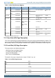
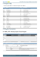
7.4 Register Map
The offset register address is relative to the registers base address.
Offset Name Type Description
0x000 MSC_CTRL RW Memory System Control Register
0x004 MSC_READCTRL RW Read Control Register
0x008 MSC_WRITECTRL RW Write Control Register
0x00C MSC_WRITECMD W1 Write Command Register
0x010 MSC_ADDRB RW Page Erase/Write Address Buffer
0x018 MSC_WDATA RW Write Data Register
0x01C MSC_STATUS R Status Register
0x02C MSC_IF R Interrupt Flag Register
0x030 MSC_IFS W1 Interrupt Flag Set Register
0x034 MSC_IFC W1 Interrupt Flag Clear Register
0x038 MSC_IEN RW Interrupt Enable Register
0x03C MSC_LOCK RW Configuration Lock Register
0x040 MSC_CMD W1 Command Register
0x044 MSC_CACHEHITS R Cache Hits Performance Counter
0x048 MSC_CACHEMISSES R Cache Misses Performance Counter
0x050 MSC_TIMEBASE RW Flash Write and Erase Timebase
0x054 MSC_MASSLOCK RW Mass Erase Lock Register
7.5 Register Description
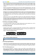
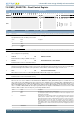
7.5.1 MSC_CTRL - Memory System Control Register
Offset Bit Position
0x000
31
30
29
28
27
26
25
24
23
22
21
20
19
18
17
16
15
14
13
12
11
10
9
8
7
6
5
4
3
2
1
0
Reset
1
Access
RW
Name
BUSFAULT
Bit Name Reset Access Description
31:1 Reserved
To ensure compatibility with future devices, always write bits to 0. More information in Section 2.1 (p. 3)
0 BUSFAULT 1 RW Bus Fault Response Enable
When this bit is set, the memory system generates bus error response
Value Mode Description
0 GENERATE A bus fault is generated on access to unmapped code and system space
1 IGNORE Accesses to unmapped address space is ignored