
User manual

...the world's most energy friendly microcontrollers
2012-04-24 - Giant Gecko Family - d0053_Rev0.96 34
www.energymicro.com
There are 32 page lock bits per page lock word (PLW). Bit 0 refers to the first page and bit 31 refers
to the last page within a PLW. Thus, PLW[0] contains lock bits for page 0-31 in the main block, PLW[1]
contains lock bits for page 32-63 etc. A page is locked when the bit is 0. A locked page cannot be erased
or written.
Word 127 is the debug lock word (DLW). The four LSBs of this word are the debug lock bits. If these bits
are 0xF, then debug access is enabled. Debug access to the core is disabled from power-on reset until
the DLW is evaluated immediately before the Cortex-M3 starts execution of the user application code.
If the bits are not 0xF, then debug access to the core remains blocked.
Word 126 is the user page lock word (ULW). Bit 0 of this word is the User Data Page lock bit. Bit 1 in
this word locks the Lock Bits Page. The lock bits can be reset by a device erase operation initiated from
the Authentication Access Port (AAP) registers. The AAP is described in more detail in Section 6.4 (p.
27) . Note that the AAP is only accessible from the debug interface, and cannot be accessed from the
Cortex-M3 core.
Word 125 is the mass erase lock word (MLW). For devices that support read-while-write, bit 0 locks the
lower half of the flash, preventing mass erase, and bit 1 locks the upper half of the flash. For devices
that do not support read-while-write, bit 0 locks the entire flash. The mass erase lock bits will not have
any effect on device erases initiated from the Authenitcation Access Port (AAP) registers. The AAP is
described in more detail in Section 6.4 (p. 27) .
7.3.3 Device Information (DI) Page
This read-only page holds oscillator, DAC and ADC calibration data from the production test as well as
an unique device ID. The page is further described in Section 5.6 (p. 23) .
7.3.4 Device Revision
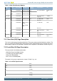
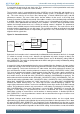
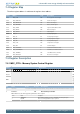
The device revision number is read from the ROM Table. The Revision number is extracted from the
PID2 and PID3 registers, as illustrated in Figure 7.1 (p. 34) .The Rev[7:4] and Rev[3:0] must be
combined to form the complete revision number Revision[7:0].
Figure 7.1. Revision Number Extraction
PID3 (0xE0 0FFFEC)
31:8 7:4
3:0
Rev[3:0]
PID2 (0xE0 0FFFE8)
31:8 7:4
3:0
Rev[7:4]
The Revision number is to be interpreted according to Table 7.3 (p. 34) .
Table 7.3. Revision Number Interpretation
Revision[7:0] Revision
0x00 A
7.3.5 Post-reset Behavior
Calibration values are automatically written to registers by the MSC before application code startup. The
values are also available to read from the DI page for later reference by software. Other information
such as the device ID and production date is also stored in the DI page and is readable from software.
7.3.5.1 One Wait-state Access
After reset, the HFCORECLK is normally 14 MHz from the HFRCO and the MODE field of the
MSC_READCTRL register is set to WS1 (one wait-state). The reset value must be WS1 as an
uncalibrated HFRCO may produce a frequency higher than 16 MHz. Software must not select a zero
wait-state mode unless the clock is guaranteed to be 16 MHz or below, otherwise the resulting behavior