
User manual


...the world's most energy friendly microcontrollers
2012-04-24 - Giant Gecko Family - d0053_Rev0.96 29
www.energymicro.com
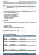
6.5 Register Map
The offset register address is relative to the registers base address.
Offset Name Type Description
0x000 AAP_CMD W1 Command Register
0x004 AAP_CMDKEY W1 Command Key Register
0x008 AAP_STATUS R Status Register
0x0FC AAP_IDR R AAP Identification Register
6.6 Register Description
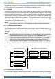
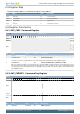
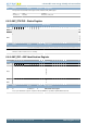
6.6.1 AAP_CMD - Command Register
Offset Bit Position
0x000
31
30
29
28
27
26
25
24
23
22
21
20
19
18
17
16
15
14
13
12
11
10
9
8
7
6
5
4
3
2
1
0
Reset
0
0
Access
W1
W1
Name
SYSRESETREQ
DEVICEERASE
Bit Name Reset Access Description
31:2 Reserved
To ensure compatibility with future devices, always write bits to 0. More information in Section 2.1 (p. 3)
1 SYSRESETREQ 0 W1 System Reset Request
A system reset request is generated when set to 1. This register is write enabled from the AAP_CMDKEY register.
0 DEVICEERASE 0 W1 Erase the Flash Main Block, SRAM and Lock Bits
When set, all data and program code in the main block is erased, the SRAM is cleared and then the Lock bit (LB) page is erased.
This also includes the Debug lock word (DLW), causing debug access to be enabled after the next reset. The information block
user data page (UD) is left unchanged, but the User data page lock word (ULW) is erased. This register is write enabled from the
AAP_CMDKEY register.
6.6.2 AAP_CMDKEY - Command Key Register
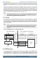
Offset Bit Position
0x004
31
30
29
28
27
26
25
24
23
22
21
20
19
18
17
16
15
14
13
12
11
10
9
8
7
6
5
4
3
2
1
0
Reset
0x00000000
Access
W1
Name
WRITEKEY
Bit Name Reset Access Description
31:0 WRITEKEY 0x00000000 W1 CMD Key Register